 |
전자부품 데이터시트 검색엔진 |
|
|
전자부품 데이터시트 검색엔진 |
|
The question interval is too short.
Please try again in a few seconds.

Hello, Please ask a question about GD25LE64CSJS Datasheet
# Example questions:
➢ What are the primary functions of the following pins: so, si, sck, and wp?
➢ Describe how the 'hold' pin functions and what conditions must be met for it to properly suspend communication with the device.
➢ If the status register is configured with bp4=0, bp3=1, bp2=1, bp1=1, and bp0=0, what portion of the memory is protected?
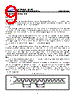
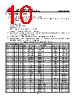
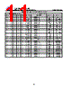
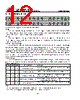
| Part No. | GD25LE64CSJS |
| Manufacturer | GIGADEVICE |
| Size | 1Mb |
| Pages | 79 pages |
| Description | 1.8V Uniform Sector Dual and Quad Serial Flash |


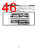
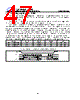
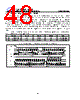
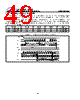

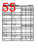
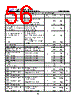
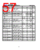
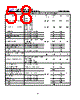
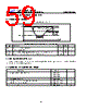
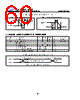
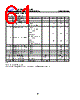
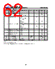

| Part No. | GD25LE64CSJS |
| Manufacturer | GIGADEVICE |
| Size | 1Mb |
| Pages | 79 pages |
| Description | 1.8V Uniform Sector Dual and Quad Serial Flash |
| ALLDATASHEET 가 귀하에 도움이 되셨나요? [ DONATE ] |
Alldatasheet는? | 광고문의 | 운영자에게 연락하기 | 개인정보취급방침 | 링크 투 데이터시트 | 링크교환 | 제조사별 검색 All Rights Reserved©Alldatasheet.com |
| Russian : Alldatasheetru.com | Korean : Alldatasheet.co.kr | Spanish : Alldatasheet.es | French : Alldatasheet.fr | Italian : Alldatasheetit.com Portuguese : Alldatasheetpt.com | Polish : Alldatasheet.pl | Vietnamese : Alldatasheet.vn Indian : Alldatasheet.in | Mexican : Alldatasheet.com.mx | British : Alldatasheet.co.uk | New Zealand : Alldatasheet.co.nz |
|
Family Site : ic2ic.com |
icmetro.com |
 Korean ▼
  English
 Chinese
 German
 Japanese
 Russian
 Spanish
 French
 Italian
 Portuguese
 Polish
 Vietnamese
 Indian
 Mexican
 British
 New Zealand