 |
전자부품 데이터시트 검색엔진 |
|
|
전자부품 데이터시트 검색엔진 |
|
The question interval is too short.
Please try again in a few seconds.

Hello, Please ask a question about MAX5141 Datasheet
# Example questions:
➢ What are the values and types of capacitors suggested, and what purpose does each serve?
➢ What is the primary difference in the clearing behavior of the max5141/max5143 compared to the max5142/max5144 when a logic low pulse is applied to the clr pin?
➢ What is the recommended maximum input impedance for the external voltage reference to maintain 14-bit accuracy, and why is this important?
| Part No. | MAX5141 |
| Manufacturer | MAXIM |
| Size | 410 Kbytes |
| Pages | 12 pages |
| Description | +3V/+5V, Serial-Input, Voltage-Output, 14-Bit DACs |


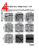
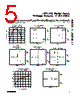
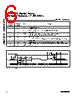
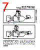


1. General Description & Functionality
️· What they are: Voltage-output, 14-bit digital-to-analog converters (DACs).
️· Key Features:
- Full 14-bit performance (less than 1 LSB integral and differential linearity error).
- Serial data interface (minimizes pin count).
- Compatible with SPI/QSPI/MICROWIRE interfaces.
- Asynchronous clear function.
- Power-on reset function ensures predictable initial state.
️· Models: MAX5141, MAX5142, MAX5143, MAX5144. The key differences are in the clear functionality (code 0 vs. code 8192) and the options for bipolar output.
2. Digital Interface
️· Serial Communication: Uses a 3-wire interface (CS, SCLK, DIN).
️· Chip Select (CS): Frames the serial data. Data is latched on the rising edge of SCLK after CS goes low.
️· Serial Clock (SCLK): Synchronizes data input. Duty cycle must be between 50%.
️· Data Input (DIN): Receives serial data. Requires 16 bits (14 data bits + 2 zero sub-bits).
️· Data Transfer: 16 bits of data must be transferred after the CS goes low.
3. Clearing the DAC
️· CLR Input: A logic-low pulse on the CLR input clears the DAC.
- MAX5141/MAX5143: Clears to code 0.
- MAX5142/MAX5144: Clears to code 8192.
4. Reference & Power
️· Reference Voltage: Operates with external voltage references from +2V to VDD (supply voltage).
️· Supply Voltage:
- MAX5143/MAX5144: +3V
- MAX5141/MAX5142: +5V
️· Reference Considerations: Reference voltage should ideally have a temperature coefficient of < 0.5 ppm/°C. Low impedance reference is critical for performance.
5. Applications and Considerations
️· Bipolar Operation: The MAX5142 and MAX5144 have matched bipolar offset resistors for use with external op-amps.
️· Reference Impedance: The input resistance seen by the reference voltage is code-dependent and varies. Maintaining a low-impedance reference is important to prevent errors.
️· Bypassing: Ceramic capacitors are recommended for high frequency bypassing of the reference voltage, and a low-ESR capacitor for low-frequency bypassing.
6. Pin Descriptions (Key Ones)
️· REF: Voltage Reference Input
️· CS: Chip Select Input
️· SCLK: Serial Clock Input
️· DIN: Serial Data Input
️· CLR: Clear Input
️· OUT: DAC Output Voltage
️· INV/RFB: Connections used for external op amp in bipolar output configuration.
️· VDD/GND: Supply voltage and ground.
1. General Description & Functionality
️· What they are: Voltage-output, 14-bit digital-to-analog converters (DACs).
️· Key Features:
- Full 14-bit performance (less than 1 LSB integral and differential linearity error).
- Serial data interface (minimizes pin count).
- Compatible with SPI/QSPI/MICROWIRE interfaces.
- Asynchronous clear function.
- Power-on reset function ensures predictable initial state.
️· Models: MAX5141, MAX5142, MAX5143, MAX5144. The key differences are in the clear functionality (code 0 vs. code 8192) and the options for bipolar output.
2. Digital Interface
️· Serial Communication: Uses a 3-wire interface (CS, SCLK, DIN).
️· Chip Select (CS): Frames the serial data. Data is latched on the rising edge of SCLK after CS goes low.
️· Serial Clock (SCLK): Synchronizes data input. Duty cycle must be between 50%.
️· Data Input (DIN): Receives serial data. Requires 16 bits (14 data bits + 2 zero sub-bits).
️· Data Transfer: 16 bits of data must be transferred after the CS goes low.
3. Clearing the DAC
️· CLR Input: A logic-low pulse on the CLR input clears the DAC.
- MAX5141/MAX5143: Clears to code 0.
- MAX5142/MAX5144: Clears to code 8192.
4. Reference & Power
️· Reference Voltage: Operates with external voltage references from +2V to VDD (supply voltage).
️· Supply Voltage:
- MAX5143/MAX5144: +3V
- MAX5141/MAX5142: +5V
️· Reference Considerations: Reference voltage should ideally have a temperature coefficient of < 0.5 ppm/°C. Low impedance reference is critical for performance.
5. Applications and Considerations
️· Bipolar Operation: The MAX5142 and MAX5144 have matched bipolar offset resistors for use with external op-amps.
️· Reference Impedance: The input resistance seen by the reference voltage is code-dependent and varies. Maintaining a low-impedance reference is important to prevent errors.
️· Bypassing: Ceramic capacitors are recommended for high frequency bypassing of the reference voltage, and a low-ESR capacitor for low-frequency bypassing.
6. Pin Descriptions (Key Ones)
️· REF: Voltage Reference Input
️· CS: Chip Select Input
️· SCLK: Serial Clock Input
️· DIN: Serial Data Input
️· CLR: Clear Input
️· OUT: DAC Output Voltage
️· INV/RFB: Connections used for external op amp in bipolar output configuration.
️· VDD/GND: Supply voltage and ground.
| Part No. | MAX5141 |
| Manufacturer | MAXIM |
| Size | 410 Kbytes |
| Pages | 12 pages |
| Description | +3V/+5V, Serial-Input, Voltage-Output, 14-Bit DACs |
| ALLDATASHEET 가 귀하에 도움이 되셨나요? [ DONATE ] |
Alldatasheet는? | 광고문의 | 운영자에게 연락하기 | 개인정보취급방침 | 링크 투 데이터시트 | 링크교환 | 제조사별 검색 All Rights Reserved©Alldatasheet.com |
| Russian : Alldatasheetru.com | Korean : Alldatasheet.co.kr | Spanish : Alldatasheet.es | French : Alldatasheet.fr | Italian : Alldatasheetit.com Portuguese : Alldatasheetpt.com | Polish : Alldatasheet.pl | Vietnamese : Alldatasheet.vn Indian : Alldatasheet.in | Mexican : Alldatasheet.com.mx | British : Alldatasheet.co.uk | New Zealand : Alldatasheet.co.nz |
|
Family Site : ic2ic.com |
icmetro.com |
 Korean ▼
  English
 Chinese
 German
 Japanese
 Russian
 Spanish
 French
 Italian
 Portuguese
 Polish
 Vietnamese
 Indian
 Mexican
 British
 New Zealand