|
전자부품 데이터시트 검색엔진 |
|
|
전자부품 데이터시트 검색엔진 |
|
TMS320DM814x 데이터시트(PDF) 314 Page - Texas Instruments |
|
|
|||||||||||||||||||||||||||||
TMS320DM814x 데이터시트(HTML) 314 Page - Texas Instruments |
|
|
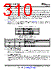
314 / 376 page  A1 A2 Processor Differential Clock Output Buffer DDR Differential CK Input Buffers Routed as Differential Pair A3 AT Rcp Clock Parallel Terminator A1 A2 A3 AT Rcp Cac DDR_1V5 0.1 µF + – + – + – = Rtt A2 A3 A4 AT Vtt A3 TMS320DM8148, TMS320DM8147 SPRS647E – MARCH 2011 – REVISED DECEMBER 2013 www.ti.com Figure 8-63. ADDR_CTRL Routing for Four Mirrored DDR3 Devices 8.13.4.2.4.11.4 Two DDR3 Devices Two DDR3 devices are supported on the DDR EMIF consisting of two x8 DDR3 devices arranged as one bank (CS), 16-bits wide, or two x16 DDR3 devices arranged as one bank (CS), 32-bits wide. These two devices may be mounted on a single side of the PCB, or may be mirrored in a pair to save board space at a cost of increased routing complexity and parts on the backside of the PCB. 8.13.4.2.4.11.5 CK and ADDR_CTRL Topologies, Two DDR3 Devices Figure 8-64 shows the topology of the CK net classes and Figure 8-65 shows the topology for the corresponding ADDR_CTRL net classes. Figure 8-64. CK Topology for Two DDR3 Devices 314 Peripheral Information and Timings Copyright © 2011–2013, Texas Instruments Incorporated Submit Documentation Feedback Product Folder Links: TMS320DM8148 TMS320DM8147 |
|
링크 URL |
| ALLDATASHEET 가 귀하에 도움이 되셨나요? [ DONATE ] |
Alldatasheet는? | 광고문의 | 운영자에게 연락하기 | 개인정보취급방침 | 링크 투 데이터시트 | 링크교환 | 제조사별 검색 All Rights Reserved©Alldatasheet.com |
| Russian : Alldatasheetru.com | Korean : Alldatasheet.co.kr | Spanish : Alldatasheet.es | French : Alldatasheet.fr | Italian : Alldatasheetit.com Portuguese : Alldatasheetpt.com | Polish : Alldatasheet.pl | Vietnamese : Alldatasheet.vn Indian : Alldatasheet.in | Mexican : Alldatasheet.com.mx | British : Alldatasheet.co.uk | New Zealand : Alldatasheet.co.nz |
|
Family Site : ic2ic.com |
icmetro.com |
 Korean ▼
 English
 Chinese
 German
 Japanese
 Russian
 Korean
 Spanish
 French
 Italian
 Portuguese
 Polish
 Vietnamese
 Indian
 Mexican
 British
 New Zealand