 |
전자부품 데이터시트 검색엔진 |
|
|
전자부품 데이터시트 검색엔진 |
|
The question interval is too short.
Please try again in a few seconds.

Hello, Please ask a question about ACT4060A Datasheet
# Example questions:
➢ The document provides a bill of materials (bom) for a 3v output application. besides specifying the part, what other key characteristics are listed for the inductor (l1) in the bom?
➢ The document details a step-by-step process for compensating the ic. what is the first step in this process, and what is its purpose?
➢ What are the key considerations when selecting an inductor (l1) for the act4060a application circuit?
| Part No. | ACT4060A |
| Manufacturer | ACTIVE-SEMI |
| Size | 257 Kbytes |
| Pages | 12 pages |
| Description | Wide Input 2A Step Down Converter |


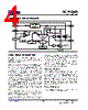

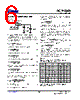
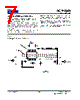


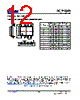

1. Overview & Intended Use
️· The ACT4060A is a synchronous buck switching regulator. This means it's designed to step down a DC voltage to a lower DC voltage efficiently. It's suitable for applications requiring regulated power.
️· It features synchronous rectification, which significantly improves efficiency compared to traditional diode-based buck converters.
2. Key Features & Benefits
️· Synchronous Rectification: Higher efficiency, reduces power losses.
️· Integrated Power MOSFETs: Simplifies design and reduces component count.
️· Wide Input Voltage Range: Likely to handle a variety of input voltages (specific range not explicitly stated, but implied to be broad).
️· Adjustable Switching Frequency: Allows optimization of efficiency and component size.
️· Current Limit Protection: Protects the regulator and load from overcurrent conditions.
️· Thermal Shutdown Protection: Prevents damage from overheating.
️· Soft-Start: Limits inrush current during startup.
3. Design Considerations & Components
️· Input Capacitor (C1): Critical for filtering input voltage ripple and providing a stable input voltage to the regulator. A ceramic capacitor is recommended.
️· Output Capacitor (C4): Important for filtering output voltage ripple and providing dynamic stability. The type (ceramic, SP-CAP) depends on application needs. SP-CAPs offer good characteristics.
️· Inductor (L1): Select an inductor with appropriate saturation current (ISAT) and DC resistance (DCR) to meet efficiency and current requirements.
️· Schottky Diode (D1): Used as part of the synchronous rectification path. Needs to handle the voltage and current requirements. (e.g., 40V, 3A)
️· Resistors (R1, R2, R3): Used for setting feedback voltage and compensation. Exact values depend on the desired output voltage and stability requirements.
️· Feedback Network: Proper compensation is crucial for stability. The documentation includes guidelines on setting the crossover frequency and the use of C2 and C3 for compensation.
4. Design Steps (Summary of Process)
1. Set the Output Voltage: Design the feedback network (R1, R2) to achieve the desired output voltage.
2. Select the Switching Frequency: Optimize for efficiency and component size.
3. Calculate Inductor Value: Based on switching frequency, input voltage range, and output voltage.
4. Choose Output Capacitor: Select based on ripple requirements and stability.
5. Design the Compensation Network (C2, C3): Ensure stability. The crossover frequency should be set at 1/10 of the switching frequency.
6. PCB Layout: Follow the layout guidelines carefully (see below).
5. PCB Layout Guidelines (Critical)
️· Short, Wide Traces: Minimize trace lengths and use wide traces for power paths to reduce resistance.
️· Ground Plane: Use a ground plane to minimize noise and improve heat dissipation.
️· Separate Switching Current Loop: Minimize the area of the switching current loop.
️· Minimize Noise-Sensitive Traces: Keep feedback and compensation traces away from noisy components.
️· Placement: Place components close to the IC. Ceramic input capacitor (C1) should be placed as close as possible to the IC's V IN and GND pins.
️· Multiple Vias: Use multiple vias to connect power planes.
6. Compensation Details
️· Crossover Frequency: Set to 1/10 of the switching frequency.
️· Use R1 and R2 to set output voltage
️· C2 and C3 for compensation
7. Bill of Materials (Example for 3.3V Output)
The documentation provides a sample BOM for a 3.3V/2A output application, including specific component recommendations. It is important to review this carefully and select components that meet your application's specific requirements.
1. Overview & Intended Use
️· The ACT4060A is a synchronous buck switching regulator. This means it's designed to step down a DC voltage to a lower DC voltage efficiently. It's suitable for applications requiring regulated power.
️· It features synchronous rectification, which significantly improves efficiency compared to traditional diode-based buck converters.
2. Key Features & Benefits
️· Synchronous Rectification: Higher efficiency, reduces power losses.
️· Integrated Power MOSFETs: Simplifies design and reduces component count.
️· Wide Input Voltage Range: Likely to handle a variety of input voltages (specific range not explicitly stated, but implied to be broad).
️· Adjustable Switching Frequency: Allows optimization of efficiency and component size.
️· Current Limit Protection: Protects the regulator and load from overcurrent conditions.
️· Thermal Shutdown Protection: Prevents damage from overheating.
️· Soft-Start: Limits inrush current during startup.
3. Design Considerations & Components
️· Input Capacitor (C1): Critical for filtering input voltage ripple and providing a stable input voltage to the regulator. A ceramic capacitor is recommended.
️· Output Capacitor (C4): Important for filtering output voltage ripple and providing dynamic stability. The type (ceramic, SP-CAP) depends on application needs. SP-CAPs offer good characteristics.
️· Inductor (L1): Select an inductor with appropriate saturation current (ISAT) and DC resistance (DCR) to meet efficiency and current requirements.
️· Schottky Diode (D1): Used as part of the synchronous rectification path. Needs to handle the voltage and current requirements. (e.g., 40V, 3A)
️· Resistors (R1, R2, R3): Used for setting feedback voltage and compensation. Exact values depend on the desired output voltage and stability requirements.
️· Feedback Network: Proper compensation is crucial for stability. The documentation includes guidelines on setting the crossover frequency and the use of C2 and C3 for compensation.
4. Design Steps (Summary of Process)
1. Set the Output Voltage: Design the feedback network (R1, R2) to achieve the desired output voltage.
2. Select the Switching Frequency: Optimize for efficiency and component size.
3. Calculate Inductor Value: Based on switching frequency, input voltage range, and output voltage.
4. Choose Output Capacitor: Select based on ripple requirements and stability.
5. Design the Compensation Network (C2, C3): Ensure stability. The crossover frequency should be set at 1/10 of the switching frequency.
6. PCB Layout: Follow the layout guidelines carefully (see below).
5. PCB Layout Guidelines (Critical)
️· Short, Wide Traces: Minimize trace lengths and use wide traces for power paths to reduce resistance.
️· Ground Plane: Use a ground plane to minimize noise and improve heat dissipation.
️· Separate Switching Current Loop: Minimize the area of the switching current loop.
️· Minimize Noise-Sensitive Traces: Keep feedback and compensation traces away from noisy components.
️· Placement: Place components close to the IC. Ceramic input capacitor (C1) should be placed as close as possible to the IC's V IN and GND pins.
️· Multiple Vias: Use multiple vias to connect power planes.
6. Compensation Details
️· Crossover Frequency: Set to 1/10 of the switching frequency.
️· Use R1 and R2 to set output voltage
️· C2 and C3 for compensation
7. Bill of Materials (Example for 3.3V Output)
The documentation provides a sample BOM for a 3.3V/2A output application, including specific component recommendations. It is important to review this carefully and select components that meet your application's specific requirements.
| Part No. | ACT4060A |
| Manufacturer | ACTIVE-SEMI |
| Size | 257 Kbytes |
| Pages | 12 pages |
| Description | Wide Input 2A Step Down Converter |
| ALLDATASHEET 가 귀하에 도움이 되셨나요? [ DONATE ] |
Alldatasheet는? | 광고문의 | 운영자에게 연락하기 | 개인정보취급방침 | 링크 투 데이터시트 | 링크교환 | 제조사별 검색 All Rights Reserved©Alldatasheet.com |
| Russian : Alldatasheetru.com | Korean : Alldatasheet.co.kr | Spanish : Alldatasheet.es | French : Alldatasheet.fr | Italian : Alldatasheetit.com Portuguese : Alldatasheetpt.com | Polish : Alldatasheet.pl | Vietnamese : Alldatasheet.vn Indian : Alldatasheet.in | Mexican : Alldatasheet.com.mx | British : Alldatasheet.co.uk | New Zealand : Alldatasheet.co.nz |
|
Family Site : ic2ic.com |
icmetro.com |
 Korean ▼
  English
 Chinese
 German
 Japanese
 Russian
 Spanish
 French
 Italian
 Portuguese
 Polish
 Vietnamese
 Indian
 Mexican
 British
 New Zealand