|
전자부품 데이터시트 검색엔진 |
|
|
전자부품 데이터시트 검색엔진 |
|
ACT4060A 데이터시트(PDF) 2 Page - Active-Semi, Inc |
|
|
|||||||||||||||||||||||||||||
ACT4060A 데이터시트(HTML) 2 Page - Active-Semi, Inc |
|
|
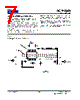
2 / 12 page  ACT4060A Rev 1, 25-Jun-09 Innovative Power TM - 2 - www.active-semi.com Copyright © 2009 Active-Semi, Inc. ORDERING INFORMATION PART NUMBER TEMPERATURE RANGE PACKAGE PINS PACKING ACT4060ASH -40°C to 85°C SOP-8 8 TUBE ACT4060ASH-T -40°C to 85°C SOP-8 8 TAPE & REEL PIN DESCRIPTIONS PIN NAME DESCRIPTION 1 BS Bootstrap. This pin acts as the positive rail for the high-side switch’s gate driver. Connect a 10nF capacitor between BS and SW. 2 IN Input Supply. Bypass this pin to G with a low ESR capacitor. See Input Capacitor in the Application Information section. 3 SW Switch Output. Connect this pin to the switching end of the inductor. 4 G Ground. 5 FB Feedback Input. The voltage at this pin is regulated to 1.293V. Connect to the resistor divider between output and ground to set output voltage. 6 COMP Compensation Pin. See Stability Compensation in the Application Information section. 7 EN Enable Input. When higher than 1.3V, this pin turns the IC on. When lower than 0.7V, this pin turns the IC off. Output voltage is discharged when the IC is off. When left unconnected, EN is pulled up to 4.5V with a 2µA pull-up current. 8 N/C Not Connected. PIN CONFIGURATION SOP-8 1 2 3 4 BS IN SW G N/C EN COMP FB ACT4060ASH 8 7 6 5 |
|
|
링크 URL |
| ALLDATASHEET 가 귀하에 도움이 되셨나요? [ DONATE ] |
Alldatasheet는? | 광고문의 | 운영자에게 연락하기 | 개인정보취급방침 | 링크 투 데이터시트 | 링크교환 | 제조사별 검색 All Rights Reserved©Alldatasheet.com |
| Russian : Alldatasheetru.com | Korean : Alldatasheet.co.kr | Spanish : Alldatasheet.es | French : Alldatasheet.fr | Italian : Alldatasheetit.com Portuguese : Alldatasheetpt.com | Polish : Alldatasheet.pl | Vietnamese : Alldatasheet.vn Indian : Alldatasheet.in | Mexican : Alldatasheet.com.mx | British : Alldatasheet.co.uk | New Zealand : Alldatasheet.co.nz |
|
Family Site : ic2ic.com |
icmetro.com |
 Korean ▼
 English
 Chinese
 German
 Japanese
 Russian
 Korean
 Spanish
 French
 Italian
 Portuguese
 Polish
 Vietnamese
 Indian
 Mexican
 British
 New Zealand