|
전자부품 데이터시트 검색엔진 |
|
|
전자부품 데이터시트 검색엔진 |
|
FP6863 데이터시트(PDF) 8 Page - Fitipower Integrated Technology Inc. |
|
|
|||||||||||||||||||||||||||||
FP6863 데이터시트(HTML) 8 Page - Fitipower Integrated Technology Inc. |
|
|
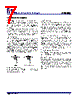
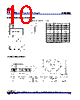
8 / 10 page  8 FP6863-1.2-FEB-2012 FP6863 85T fitipower integrated technology lnc. Application Information Input Capacitor A 1 μF or above low-ESR ceramic capacitor for input capacitor is recommended for general application. Input capacitor is not necessary for operation, but it is useful to prevent from affecting upstream circuits such as noisy supply voltage or output short. Output short circuit may cause ringing on the input terminal (from source lead inductance) to destroy the internal control circuitry. The input transient must not exceed 6V of the absolute maximum supply voltage even for a short duration. Output Capacitor A 0.1 μF or above capacitor between V OUT and GND is recommended. Standard bypass methods should be used to minimize inductance and resistance between the bypass capacitor and the downstream connector to reduce EMI and decouple voltage drop caused when downstream transients. Power Dissipation The device’s junction temperature depends on several factors such as the load, PCB layout, ambient temperature and package type. The output pin of FP6863 can deliver current up to 1.5A, respectively over the full operating junction temperature range. However, the maximum output current must be decreased at higher ambient temperature to ensure the junction temperature does not exceed 125°C. With all possible conditions, the junction temperature must be within the range specified under operating conditions. Power dissipation can be calculated based on the output current and the RDS-ON of switch as below: =R S O OUT2 Although the devices are rated for 1.5A of output current, but the application may limit the amount of output current based on the total power dissipation and the ambient temperature. The final operating junction temperature for any set of conditions can be estimated by the following thermal equation: MA )= T MA ) TA θ A Where TJ(MAX) is the maximum operation junction temperature, TA is the ambient temperature and the θ JA is the junction to ambient thermal resistance. |
|
|
링크 URL |
| ALLDATASHEET 가 귀하에 도움이 되셨나요? [ DONATE ] |
Alldatasheet는? | 광고문의 | 운영자에게 연락하기 | 개인정보취급방침 | 링크 투 데이터시트 | 링크교환 | 제조사별 검색 All Rights Reserved©Alldatasheet.com |
| Russian : Alldatasheetru.com | Korean : Alldatasheet.co.kr | Spanish : Alldatasheet.es | French : Alldatasheet.fr | Italian : Alldatasheetit.com Portuguese : Alldatasheetpt.com | Polish : Alldatasheet.pl | Vietnamese : Alldatasheet.vn Indian : Alldatasheet.in | Mexican : Alldatasheet.com.mx | British : Alldatasheet.co.uk | New Zealand : Alldatasheet.co.nz |
|
Family Site : ic2ic.com |
icmetro.com |
 Korean ▼
 English
 Chinese
 German
 Japanese
 Russian
 Korean
 Spanish
 French
 Italian
 Portuguese
 Polish
 Vietnamese
 Indian
 Mexican
 British
 New Zealand