|
전자부품 데이터시트 검색엔진 |
|
|
전자부품 데이터시트 검색엔진 |
|
GD25LQ64CSJS 데이터시트(PDF) 20 Page - GigaDevice Semiconductor (Beijing) Inc. |
|
|
|||||||||||||||||||||||||||||
GD25LQ64CSJS 데이터시트(HTML) 20 Page - GigaDevice Semiconductor (Beijing) Inc. |
|
|
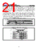
20 / 77 page  1.8V Uniform Sector Dual and Quad Serial Flash GD25LQ64C 20 Figure5. Read Status Register Sequence Diagram Command 0 1 2 3 4 5 6 7 05H or 35H CS# SCLK SI SO High-Z 8 9 10 11 12 13 14 15 7 6 5 4 3 2 1 0 7 6 5 4 3 2 1 0 7 MSB S7~S0 or S15~S8 out S7~S0 or S15~S8 out MSB Figure5a. Read Status Register Sequence Diagram (QPI) CS# SCLK IO0 IO1 IO2 IO3 0 1 2 3 4 5 Command 05H or 35H 4 4 0 0 5 5 1 1 4 5 6 2 6 2 6 7 3 7 3 7 S7-S0 or S15-S8 out Figure5b. Read Status Register Sequence Diagram (QPI) (15H) CS# SCLK IO0 IO1 IO2 IO3 0 1 2 3 4 5 Command 15H S1 S1 S0 S0 S1-S0 out 7.5 Write Status Register (WRSR) (01H) The Write Status Register (WRSR) command allows new values to be written to the Status Register. Before it can be accepted, a Write Enable (WREN) command must previously have been executed. After the Write Enable (WREN) command has been decoded and executed, the device sets the Write Enable Latch (WEL). The Write Status Register (WRSR) command has no effect on S15, S10, S1 and S0 of the Status Register. CS# must |
|
링크 URL |
| ALLDATASHEET 가 귀하에 도움이 되셨나요? [ DONATE ] |
Alldatasheet는? | 광고문의 | 운영자에게 연락하기 | 개인정보취급방침 | 링크 투 데이터시트 | 링크교환 | 제조사별 검색 All Rights Reserved©Alldatasheet.com |
| Russian : Alldatasheetru.com | Korean : Alldatasheet.co.kr | Spanish : Alldatasheet.es | French : Alldatasheet.fr | Italian : Alldatasheetit.com Portuguese : Alldatasheetpt.com | Polish : Alldatasheet.pl | Vietnamese : Alldatasheet.vn Indian : Alldatasheet.in | Mexican : Alldatasheet.com.mx | British : Alldatasheet.co.uk | New Zealand : Alldatasheet.co.nz |
|
Family Site : ic2ic.com |
icmetro.com |
 Korean ▼
 English
 Chinese
 German
 Japanese
 Russian
 Korean
 Spanish
 French
 Italian
 Portuguese
 Polish
 Vietnamese
 Indian
 Mexican
 British
 New Zealand