|
전자부품 데이터시트 검색엔진 |
|
|
전자부품 데이터시트 검색엔진 |
|
S-817B13AMC-CWC-T2 데이터시트(PDF) 11 Page - Seiko Instruments Inc |
|
|
|||||||||||||||||||||||||||||
S-817B13AMC-CWC-T2 데이터시트(HTML) 11 Page - Seiko Instruments Inc |
|
|
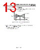
11 / 50 page  SUPER-SMALL PACKAGE CMOS VOLTAGE REGULATOR Rev.3.0_00 S-817 Series Seiko Instruments Inc. 11 Measurement Circuits 1 . VSS VOUT VIN V A + + Figure 8 2. VSS VOUT VIN A Figure 9 3. VSS VOUT VIN V A + + Figure 10 Standard Circuit VSS VOUT VIN CIN *1 CL *2 INPUT OUTPUT GND Single GND *1. CIN is a capacitor used to stabilize input. *2. A ceramic capacitor of 0.1 µF or more can be used for CL. Figure 11 Caution The above connection diagram and constant will not guarantee successful operation. Perform through evaluation using the actual application to set the constant. |
|
링크 URL |
| ALLDATASHEET 가 귀하에 도움이 되셨나요? [ DONATE ] |
Alldatasheet는? | 광고문의 | 운영자에게 연락하기 | 개인정보취급방침 | 링크 투 데이터시트 | 링크교환 | 제조사별 검색 All Rights Reserved©Alldatasheet.com |
| Russian : Alldatasheetru.com | Korean : Alldatasheet.co.kr | Spanish : Alldatasheet.es | French : Alldatasheet.fr | Italian : Alldatasheetit.com Portuguese : Alldatasheetpt.com | Polish : Alldatasheet.pl | Vietnamese : Alldatasheet.vn Indian : Alldatasheet.in | Mexican : Alldatasheet.com.mx | British : Alldatasheet.co.uk | New Zealand : Alldatasheet.co.nz |
|
Family Site : ic2ic.com |
icmetro.com |
 Korean ▼
 English
 Chinese
 German
 Japanese
 Russian
 Korean
 Spanish
 French
 Italian
 Portuguese
 Polish
 Vietnamese
 Indian
 Mexican
 British
 New Zealand