|
전자부품 데이터시트 검색엔진 |
|
|
전자부품 데이터시트 검색엔진 |
|
MC74HC393D 데이터시트(PDF) 4 Page - ON Semiconductor |
|
|
|||||||||||||||||||||||||||||
MC74HC393D 데이터시트(HTML) 4 Page - ON Semiconductor |
|
|
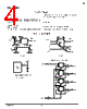
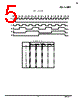
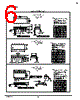
4 / 7 page  MC54/74HC393 MOTOROLA High–Speed CMOS Logic Data DL129 — Rev 6 4 PIN DESCRIPTIONS INPUTS Clock (Pins 1, 13) Clock input. The internal flip–flops are toggled and the counter state advances on high–to–low transitions of the clock input. CONTROL INPUTS Reset (Pins 2, 12) Active–high, asynchronous reset. A separate reset is pro- vided for each counter. A high at the Reset input prevents counting and forces all four outputs low. OUTPUTS Q1, Q2, Q3, Q4 (Pins 3, 4, 5, 6, 8, 9, 10, 11) Parallel binary outputs Q4 is the most significant bit. SWITCHING WAVEFORMS tPHL VCC GND VCC GND 50% 50% 50% trec CLOCK Q RESET Figure 1. Figure 2. Figure 3. Test Circuit Q1 Q2 Q3 Q4 CLOCK RESET 1, 13 2, 12 3, 11 4, 10 5, 9 6, 8 EXPANDED LOGIC DIAGRAM * Includes all probe and jig capacitance CL* TEST POINT DEVICE UNDER TEST OUTPUT CLOCK Q 90% 90% 50% 10% tf tr VCC GND tw 1/fmax tPLH tPHL 90% 50% 10% tTLH tTHL C D Q tw Q C D Q Q C D Q Q C D Q Q |
|
|
링크 URL |
| ALLDATASHEET 가 귀하에 도움이 되셨나요? [ DONATE ] |
Alldatasheet는? | 광고문의 | 운영자에게 연락하기 | 개인정보취급방침 | 링크 투 데이터시트 | 링크교환 | 제조사별 검색 All Rights Reserved©Alldatasheet.com |
| Russian : Alldatasheetru.com | Korean : Alldatasheet.co.kr | Spanish : Alldatasheet.es | French : Alldatasheet.fr | Italian : Alldatasheetit.com Portuguese : Alldatasheetpt.com | Polish : Alldatasheet.pl | Vietnamese : Alldatasheet.vn Indian : Alldatasheet.in | Mexican : Alldatasheet.com.mx | British : Alldatasheet.co.uk | New Zealand : Alldatasheet.co.nz |
|
Family Site : ic2ic.com |
icmetro.com |
 Korean ▼
 English
 Chinese
 German
 Japanese
 Russian
 Korean
 Spanish
 French
 Italian
 Portuguese
 Polish
 Vietnamese
 Indian
 Mexican
 British
 New Zealand