|
전자부품 데이터시트 검색엔진 |
|
|
전자부품 데이터시트 검색엔진 |
|
IS25LP032D-RHLA3 데이터시트(PDF) 24 Page - Integrated Silicon Solution, Inc |
|
|
|||||||||||||||||||||||||||||
IS25LP032D-RHLA3 데이터시트(HTML) 24 Page - Integrated Silicon Solution, Inc |
|
|
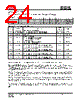
24 / 118 page  IS25LP032D IS25WP032D Integrated Silicon Solution, Inc.- www.issi.com 24 Rev. A12 08/04/2020 6.2 FUNCTION REGISTER Function Register Format and Bit definition are described in Table 6.5 and Table 6.6. Table 6.5 Function Register Format Bit 7 Bit 6 Bit 5 Bit 4 Bit 3 Bit 2 Bit 1 Bit 0 IRL3 IRL2 IRL1 IRL0 ESUS PSUS Reserved Dedicated RESET# Disable Default 0 0 0 0 0 0 0 0 or 1 Table 6.6 Function Register Bit Definition Bit Name Definition Read /Write Type Bit 0 Dedicated RESET# Disable Dedicated RESET# Disable bit “0” indicates Dedicated RESET# was enabled “1” indicates Dedicated RESET# was disabled R/W for 0 R only for 1 OTP Bit 1 Reserved Reserved R Reserved Bit 2 PSUS Program suspend bit: “0” indicates program is not suspend “1” indicates program is suspend R Volatile Bit 3 ESUS Erase suspend bit: "0" indicates Erase is not suspend "1" indicates Erase is suspend R Volatile Bit 4 IR Lock 0 Lock the Information Row 0: “0” indicates the Information Row can be programmed “1” indicates the Information Row cannot be programmed R/W OTP Bit 5 IR Lock 1 Lock the Information Row 1: “0” indicates the Information Row can be programmed “1” indicates the Information Row cannot be programmed R/W OTP Bit 6 IR Lock 2 Lock the Information Row 2: “0” indicates the Information Row can be programmed “1” indicates the Information Row cannot be programmed R/W OTP Bit 7 IR Lock 3 Lock the Information Row 3: “0” indicates the Information Row can be programmed “1” indicates the Information Row cannot be programmed R/W OTP Note: Once OTP bits of Function Register are written to “1”, it cannot be modified to “0” any more. Dedicated RESET# Disable bit: The default status of the bit is dependent on part number. The device with dedicated RESET# can be programmed to “1” to disable dedicated RESET# function to move RESET# function to Hold#/RESET# pin (or ball). So the device with dedicated RESET# can be used for dedicated RESET# application and HOLD#/RESET# application. PSUS bit: The Program Suspend Status bit indicates when a Program operation has been suspended. The PSUS changes to “1” after a suspend command is issued during the program operation. Once the suspended Program resumes, the PSUS bit is reset to “0”. ESUS bit: The Erase Suspend Status bit indicates when an Erase operation has been suspended. The ESUS bit is “1” after a suspend command is issued during an Erase operation. Once the suspended Erase resumes, the ESUS bit is reset to “0”. IR Lock bit 0 ~ 3: The default is “0” so that the Information Row can be programmed. If the bit set to “1”, the Information Row can ’t be programmed. Once it sets to “1”, it cannot be changed back to “0” since IR Lock bits are OTP. |
|
링크 URL |
| ALLDATASHEET 가 귀하에 도움이 되셨나요? [ DONATE ] |
Alldatasheet는? | 광고문의 | 운영자에게 연락하기 | 개인정보취급방침 | 링크 투 데이터시트 | 링크교환 | 제조사별 검색 All Rights Reserved©Alldatasheet.com |
| Russian : Alldatasheetru.com | Korean : Alldatasheet.co.kr | Spanish : Alldatasheet.es | French : Alldatasheet.fr | Italian : Alldatasheetit.com Portuguese : Alldatasheetpt.com | Polish : Alldatasheet.pl | Vietnamese : Alldatasheet.vn Indian : Alldatasheet.in | Mexican : Alldatasheet.com.mx | British : Alldatasheet.co.uk | New Zealand : Alldatasheet.co.nz |
|
Family Site : ic2ic.com |
icmetro.com |
 Korean ▼
 English
 Chinese
 German
 Japanese
 Russian
 Korean
 Spanish
 French
 Italian
 Portuguese
 Polish
 Vietnamese
 Indian
 Mexican
 British
 New Zealand