|
전자부품 데이터시트 검색엔진 |
|
|
전자부품 데이터시트 검색엔진 |
|
SN54LS162J 데이터시트(PDF) 5 Page - ON Semiconductor |
|
|
|||||||||||||||||||||||||||||
SN54LS162J 데이터시트(HTML) 5 Page - ON Semiconductor |
|
|
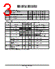
5 / 6 page  5-5 FAST AND LS TTL DATA SN54/74LS160A • SN54/74LS161A SN54/74LS162A • SN54/74LS163A AC SETUP REQUIREMENTS (TA = 25°C) Sb l P Limits Ui T C di i Symbol Parameter Min Typ Max Unit Test Conditions tWCP Clock Pulse Width Low 25 ns V5 0 V tW MR or SR Pulse Width 20 ns V5 0 V ts Setup Time, other* 20 ns V5 0 V ts Setup Time PE or SR 25 ns VCC = 5.0 V th Hold Time, data 3 ns th Hold Time, other 0 ns trec Recovery Time MR to CP 15 ns *CEP, CET or DATA DEFINITION OF TERMS SETUP TIME (ts) — is defined as the minimum time required for the correct logic level to be present at the logic input prior to the clock transition from LOW to HIGH in order to be recog- nized and transferred to the outputs. HOLD TIME (th) — is defined as the minimum time following the clock transition from LOW to HIGH that the logic level must be maintained at the input in order to ensure continued recog- nition. A negative HOLD TIME indicates that the correct logic level may be released prior to the clock transition from LOW to HIGH and still be recognized. RECOVERY TIME (trec) — is defined as the minimum time re- quired between the end of the reset pulse and the clock transi- tion from LOW to HIGH in order to recognize and transfer HIGH Data to the Q outputs. AC WAVEFORMS Figure 1. Clock to Output Delays, Count Frequency, and Clock Pulse Width Figure 2. Master Reset to Output Delay, Master Reset Pulse Width, and Master Reset Recovery Time 1.3 V 1.3 V 1.3 V 1.3 V 1.3 V 1.3 V 1.3 V CP Q tW(H) tW(L) trec tPHL tPHL tPLH OTHER CONDITIONS: PE = MR (SR) = H CEP = CET = H OTHER CONDITIONS: PE = L P0 = P1 = P2 = P3 = H tW Q0 ⋅ Q1 ⋅ Q2 ⋅ Q3 MR CP |
|
|
링크 URL |
| ALLDATASHEET 가 귀하에 도움이 되셨나요? [ DONATE ] |
Alldatasheet는? | 광고문의 | 운영자에게 연락하기 | 개인정보취급방침 | 링크 투 데이터시트 | 링크교환 | 제조사별 검색 All Rights Reserved©Alldatasheet.com |
| Russian : Alldatasheetru.com | Korean : Alldatasheet.co.kr | Spanish : Alldatasheet.es | French : Alldatasheet.fr | Italian : Alldatasheetit.com Portuguese : Alldatasheetpt.com | Polish : Alldatasheet.pl | Vietnamese : Alldatasheet.vn Indian : Alldatasheet.in | Mexican : Alldatasheet.com.mx | British : Alldatasheet.co.uk | New Zealand : Alldatasheet.co.nz |
|
Family Site : ic2ic.com |
icmetro.com |
 Korean ▼
 English
 Chinese
 German
 Japanese
 Russian
 Korean
 Spanish
 French
 Italian
 Portuguese
 Polish
 Vietnamese
 Indian
 Mexican
 British
 New Zealand