|
전자부품 데이터시트 검색엔진 |
|
|
전자부품 데이터시트 검색엔진 |
|
STPD01 데이터시트(PDF) 3 Page - STMicroelectronics |
|
|
|||||||||||||||||||||||||||||
STPD01 데이터시트(HTML) 3 Page - STMicroelectronics |
|
|
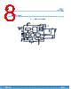
3 / 43 page  2 Pin configuration (top through view) Figure 2. Pin configuration (top through view) 1 7 19 13 20 24 12 8 Table 2. Pin description Position Name Description 1 SDA I2C data 2 SCL I2C clock 3 ADD I2C address selection (cannot be left floating) 4 INT Interrupt pin (open drain output) 5 EN Enable pin. Internally pulled up to VREG 6 VDRIVEH High-side driver supply. Connect to a bypass capacitor 7 VCC Analog supply input 8 PVIN Power supply input 9 PVIN Power supply input 10 PGND Power ground 11 PGND Power ground 12 PGND Power ground 13 LX Switching node 14 LX Switching node 15 LX Switching node 16 BOOT Connect the bootstrap capacitor (0.1 µF) between this pin and LX 17 Pon Power-on (open drain output). Pulled high when Vout reaches the regulation value after startup 18 VREG Internal LDO regulator voltage pin (connect 1 μF capacitor between this pin and GND) 19 ISNS+ Positive connection for the current sensing resistor. Connect to GND if not used 20 ISNS- Negative connection for the current sensing resistor. Connect to GND if not used 21 VSNS Output voltage sensing pin. Used also for cable drop compensation see Section 7.2 Cable drop compensation 22 CDC Cable drop compensation programming pin STPD01 Pin configuration (top through view) DS13473 - Rev 1 page 3/43 |
|
링크 URL |
| ALLDATASHEET 가 귀하에 도움이 되셨나요? [ DONATE ] |
Alldatasheet는? | 광고문의 | 운영자에게 연락하기 | 개인정보취급방침 | 링크 투 데이터시트 | 링크교환 | 제조사별 검색 All Rights Reserved©Alldatasheet.com |
| Russian : Alldatasheetru.com | Korean : Alldatasheet.co.kr | Spanish : Alldatasheet.es | French : Alldatasheet.fr | Italian : Alldatasheetit.com Portuguese : Alldatasheetpt.com | Polish : Alldatasheet.pl | Vietnamese : Alldatasheet.vn Indian : Alldatasheet.in | Mexican : Alldatasheet.com.mx | British : Alldatasheet.co.uk | New Zealand : Alldatasheet.co.nz |
|
Family Site : ic2ic.com |
icmetro.com |
 Korean ▼
 English
 Chinese
 German
 Japanese
 Russian
 Korean
 Spanish
 French
 Italian
 Portuguese
 Polish
 Vietnamese
 Indian
 Mexican
 British
 New Zealand