|
전자부품 데이터시트 검색엔진 |
|
|
전자부품 데이터시트 검색엔진 |
|
PL611-30XXXSI-R 데이터시트(PDF) 5 Page - PhaseLink Corporation |
|
|
|||||||||||||||||||||||||||||
PL611-30XXXSI-R 데이터시트(HTML) 5 Page - PhaseLink Corporation |
|
|
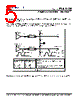
5 / 7 page  Preliminary PL611-30 Programmable Quick Turn ClockTM 47745 Fremont Blvd., Fremont, California 94538 Tel (510) 492-0990 Fax (510) 492-0991 www.phaselink.com Rev 03/03/05 Page 5 Figure 1 below describes how to terminate the differential CMOS outputs of PhaseLink’s PL611-30 Programmable QTC clock for use with PECL or LVDS inputs. The unique feature of differential CMOS outputs allows great flexibility for board designers. By standardizing on one termination scheme you can use the PL611-30 for all your LVDS and PECL clock requirements up to 375MHz. 50 Ω line 50 Ω line R3 R1 R1 R2 R2 R3 CMOS Output Complementary CMOS Output 0V 3.3V 1.59V 2.35V +3.3V +3.3V Complementary Input Input Component selection For LVDS input R1 = 360 Ω R2 = 82 Ω R3 = 130 Ω For PECL input R1 = 130 Ω R2 = 82 Ω R3 = 130 Ω Notes: Place R1 as close to the CMOS outputs as possible. Place R2 and R3 as close to the PECL/LVDS inputs as possible. PECL 1.10V 1.40V LVDS Figure 1 The above layout allows the PL611-30 to drive either a PECL or LVDS input by simply changing the value of R1. |
|
|
링크 URL |
| ALLDATASHEET 가 귀하에 도움이 되셨나요? [ DONATE ] |
Alldatasheet는? | 광고문의 | 운영자에게 연락하기 | 개인정보취급방침 | 링크 투 데이터시트 | 링크교환 | 제조사별 검색 All Rights Reserved©Alldatasheet.com |
| Russian : Alldatasheetru.com | Korean : Alldatasheet.co.kr | Spanish : Alldatasheet.es | French : Alldatasheet.fr | Italian : Alldatasheetit.com Portuguese : Alldatasheetpt.com | Polish : Alldatasheet.pl | Vietnamese : Alldatasheet.vn Indian : Alldatasheet.in | Mexican : Alldatasheet.com.mx | British : Alldatasheet.co.uk | New Zealand : Alldatasheet.co.nz |
|
Family Site : ic2ic.com |
icmetro.com |
 Korean ▼
 English
 Chinese
 German
 Japanese
 Russian
 Korean
 Spanish
 French
 Italian
 Portuguese
 Polish
 Vietnamese
 Indian
 Mexican
 British
 New Zealand