|
전자부품 데이터시트 검색엔진 |
|
|
전자부품 데이터시트 검색엔진 |
|
PLL502-26SC-R 데이터시트(PDF) 2 Page - PhaseLink Corporation |
|
|
|||||||||||||||||||||||||||||
PLL502-26SC-R 데이터시트(HTML) 2 Page - PhaseLink Corporation |
|
|
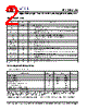
2 / 5 page  PLL502-26 High Pull-Range VCXO (27MHz) with integrated Audio PLL 47745 Fremont Blvd., Fremont, California 94538 Tel (510) 492-0990 Fax (510) 492-0991 www.phaselink.com Rev 09/17/04 Page 2 PIN DESCRIPTIONS Name Number Type Description N/C 1,16 No connection. VDD_PLL 2 P VDD power supply pin for PLL circuitry. This pin should be decoupled sepa- rately from other VDD. VDD_VCXO 3 P VDD power supply pin for VCXO circuitry. This pin should be decoupled separately from other VDD. XIN 4 I Crystal input. See Crystal Specifications on page 4. XOUT 5 O Crystal output. See Crystal Specifications on page 4. VCON 6 I Voltage Control input. GND_VCXO 7 P GND connection for VCXO circuitry. GND_PLL 8 P GND connection for VCXO circuitry. REF_Audio 9 I Audio Reference Clock input. GND_Audio 10 P GND connection for Audio clock output buffer circuitry. OUT_Audio 11 O Audio clock output. VDD_Audio 12 P VDD power supply pin for Audio clock output buffer. This pin should be decoupled separately from other VDD. VDD_27MHz 13 P VDD power supply pin for 27MHz output clock. This pin should be decoup- led separately from other VDD. OUT_27MHz 14 O 27MHz VCXO output clock. GND_27MHz 15 P GND connection for 27MHz output buffer circuitry. ELECTRICAL SPECIFICATIONS 1. Absolute Maximum Ratings PARAMETERS SYMBOL MIN. MAX. UNITS Supply Voltage VDD 4.6 V Input Voltage, dc VI -0.5 VDD+0.5 V Output Voltage, dc VO -0.5 VDD+0.5 V Storage Temperature TS -65 150 °C Ambient Operating Temperature* TA -40 85 °C Junction Temperature TJ 125 °C Lead Temperature (soldering, 10s) 260 °C ESD Protection, Human Body Model 2 kV Exposure of the device under conditions beyond the limits specified by Maximum Ratings for extended periods may cause permanent damage to the device and affect product reliability. These conditions represent a stress rating only, and functional operations of the device at these or any other conditions above the operational limits noted in this specification is not implied. * Note: Operating Temperature is guaranteed by design for all parts (COMMERCIAL and INDUSTRIAL), but tested for COMMERCIAL grade only. |
|
|
링크 URL |
| ALLDATASHEET 가 귀하에 도움이 되셨나요? [ DONATE ] |
Alldatasheet는? | 광고문의 | 운영자에게 연락하기 | 개인정보취급방침 | 링크 투 데이터시트 | 링크교환 | 제조사별 검색 All Rights Reserved©Alldatasheet.com |
| Russian : Alldatasheetru.com | Korean : Alldatasheet.co.kr | Spanish : Alldatasheet.es | French : Alldatasheet.fr | Italian : Alldatasheetit.com Portuguese : Alldatasheetpt.com | Polish : Alldatasheet.pl | Vietnamese : Alldatasheet.vn Indian : Alldatasheet.in | Mexican : Alldatasheet.com.mx | British : Alldatasheet.co.uk | New Zealand : Alldatasheet.co.nz |
|
Family Site : ic2ic.com |
icmetro.com |
 Korean ▼
 English
 Chinese
 German
 Japanese
 Russian
 Korean
 Spanish
 French
 Italian
 Portuguese
 Polish
 Vietnamese
 Indian
 Mexican
 British
 New Zealand