|
전자부품 데이터시트 검색엔진 |
|
|
전자부품 데이터시트 검색엔진 |
|
M95020-R 데이터시트(PDF) 16 Page - STMicroelectronics |
|
|
|||||||||||||||||||||||||||||
M95020-R 데이터시트(HTML) 16 Page - STMicroelectronics |
|
|
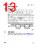
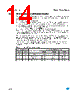
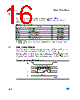
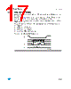
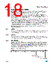
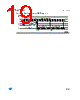
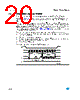
16 / 42 page  Instructions M95040, M95020, M95010 16/42 6 Instructions Each instruction starts with a single-byte code, as summarized in Table 4. If an invalid instruction is sent (one not contained in Table 4), the device automatically deselects itself. 6.1 Write Enable (WREN) The Write Enable Latch (WEL) bit must be set prior to each WRITE and WRSR instruction. The only way to do this is to send a Write Enable instruction to the device. As shown in Figure 7, to send this instruction to the device, Chip Select (S) is driven Low, and the bits of the instruction byte are shifted in, on Serial Data Input (D). The device then enters a wait state. It waits for a the device to be deselected, by Chip Select (S) being driven High. Figure 7. Write Enable (WREN) sequence Table 4. Instruction set Instruction Description Instruction Format WREN Write Enable 0000 X110(1) 1. X = Don’t Care. WRDI Write Disable 0000 X100(1) RDSR Read Status Register 0000 X101(1) WRSR Write Status Register 0000 X001(1) READ Read from Memory Array 0000 A8011 (2) 2. A8 = 1 for the upper half of the memory array of the M95040, and 0 for the lower half, and is Don’t Care for other devices. WRITE Write to Memory Array 0000 A8010 (2) C D AI01441D S Q 2 1 34567 High Impedance 0 Instruction |
|
링크 URL |
| ALLDATASHEET 가 귀하에 도움이 되셨나요? [ DONATE ] |
Alldatasheet는? | 광고문의 | 운영자에게 연락하기 | 개인정보취급방침 | 링크 투 데이터시트 | 링크교환 | 제조사별 검색 All Rights Reserved©Alldatasheet.com |
| Russian : Alldatasheetru.com | Korean : Alldatasheet.co.kr | Spanish : Alldatasheet.es | French : Alldatasheet.fr | Italian : Alldatasheetit.com Portuguese : Alldatasheetpt.com | Polish : Alldatasheet.pl | Vietnamese : Alldatasheet.vn Indian : Alldatasheet.in | Mexican : Alldatasheet.com.mx | British : Alldatasheet.co.uk | New Zealand : Alldatasheet.co.nz |
|
Family Site : ic2ic.com |
icmetro.com |
 Korean ▼
 English
 Chinese
 German
 Japanese
 Russian
 Korean
 Spanish
 French
 Italian
 Portuguese
 Polish
 Vietnamese
 Indian
 Mexican
 British
 New Zealand