|
전자부품 데이터시트 검색엔진 |
|
|
전자부품 데이터시트 검색엔진 |
|
PL611S-27-XXXTC-R 데이터시트(PDF) 6 Page - PhaseLink Corporation |
|
|
|||||||||||||||||||||||||||||
PL611S-27-XXXTC-R 데이터시트(HTML) 6 Page - PhaseLink Corporation |
|
|
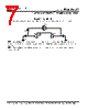
6 / 9 page  (Preliminary)PL611s-27 1.8V to 3.3V PicoPLL TM Programmable Clock 47745 Fremont Blvd., Fremont, California 94538 Tel (510) 492-0990 Fax (510) 492-0991 www.phaselink.com Rev 2/25/07 Page 6 LAYOUT RECOMMENDATIONS DFN-6L Evaluation Board The following guidelines are to assist you with a performance optimized PCB design: Signal Integrity and Termination Considerations - Keep traces short! - Trace = Inductor. With a capacitive load this equals ringing! - Long trace = Transmission Line. Without proper termination this will cause reflections ( looks like ringing ). - Design long traces as “striplines” or “microstrips” with defined impedance. - Match trace at one side to avoid reflections bouncing back and forth. Decoupling and Power Supply Considerations - Place decoupling capacitors as close as possible to the VDD pin(s) to limit noise from the power supply - Multiple VDD pins should be decoupled separately for best performance. - Addition of a ferrite bead in series with VDD can help prevent noise from other board sources - Value of decoupling capacitor is frequency dependant. Typical values to use are 0.1µF for designs using crystals < 50MHz and 0.01µF for designs using crystals > 50MHz. Typical CMOS termination Place Series Resistor as close as possible to CMOS output CMOS Output Buffer ( Typical buffer impedance 20 Ω ) To CMOS Input Series Resistor Use value to match output buffer impedance to 50 Ω trace. Typical value 30 Ω 50Ω line |
|
|
링크 URL |
| ALLDATASHEET 가 귀하에 도움이 되셨나요? [ DONATE ] |
Alldatasheet는? | 광고문의 | 운영자에게 연락하기 | 개인정보취급방침 | 링크 투 데이터시트 | 링크교환 | 제조사별 검색 All Rights Reserved©Alldatasheet.com |
| Russian : Alldatasheetru.com | Korean : Alldatasheet.co.kr | Spanish : Alldatasheet.es | French : Alldatasheet.fr | Italian : Alldatasheetit.com Portuguese : Alldatasheetpt.com | Polish : Alldatasheet.pl | Vietnamese : Alldatasheet.vn Indian : Alldatasheet.in | Mexican : Alldatasheet.com.mx | British : Alldatasheet.co.uk | New Zealand : Alldatasheet.co.nz |
|
Family Site : ic2ic.com |
icmetro.com |
 Korean ▼
 English
 Chinese
 German
 Japanese
 Russian
 Korean
 Spanish
 French
 Italian
 Portuguese
 Polish
 Vietnamese
 Indian
 Mexican
 British
 New Zealand