|
전자부품 데이터시트 검색엔진 |
|
|
전자부품 데이터시트 검색엔진 |
|
AD633JRZ-R7 데이터시트(PDF) 16 Page - Analog Devices |
|
|
|||||||||||||||||||||||||||||
AD633JRZ-R7 데이터시트(HTML) 16 Page - Analog Devices |
|
|
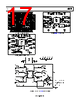
16 / 20 page  AD633 Data Sheet Rev. K | Page 16 of 20 EVALUATION BOARD The evaluation board of the AD633 enables simple bench-top experimenting to be performed with easy control of the AD633. Built-in flexibility allows convenient configuration to accommodate most operating configurations. Figure 42 is a photograph of the AD633 evaluation board. Figure 42. AD633 Evaluation Board Any dual-polarity power supply capable of providing 10 mA or greater is all that is required to perform the intended tests, in addition to whatever test equipment the user wants. Referring to the schematic in Figure 49, inputs to the multiplier are differential and dc-coupled. Three-position slide switches enhance flexibility by enabling the multiplier inputs to be connected to an active signal source, to ground, or to a test loop connected directly to the device pin for direct measurements, such as bias current. Inputs may be connected single ended or differentially, but must have a dc path to ground for bias current. If the impedance of an input source is non-zero, an equal value impedance must be connected to the opposite polarity input to avoid introducing additional offset voltage. The AD633-EVALZ can be configured for multiplier or divider operation by switch S1. Refer to Figure 16 for divider circuit connections. Figure 43 through Figure 46 are the signal, power, and ground- plane artworks, and Figure 47 shows the component and circuit side silkscreen. Figure 48 shows the assembly. Figure 43. Component Side Copper Figure 44. Circuit Side Copper Figure 45. Inner Layer Ground Plane |
|
|
링크 URL |
| ALLDATASHEET 가 귀하에 도움이 되셨나요? [ DONATE ] |
Alldatasheet는? | 광고문의 | 운영자에게 연락하기 | 개인정보취급방침 | 링크 투 데이터시트 | 링크교환 | 제조사별 검색 All Rights Reserved©Alldatasheet.com |
| Russian : Alldatasheetru.com | Korean : Alldatasheet.co.kr | Spanish : Alldatasheet.es | French : Alldatasheet.fr | Italian : Alldatasheetit.com Portuguese : Alldatasheetpt.com | Polish : Alldatasheet.pl | Vietnamese : Alldatasheet.vn Indian : Alldatasheet.in | Mexican : Alldatasheet.com.mx | British : Alldatasheet.co.uk | New Zealand : Alldatasheet.co.nz |
|
Family Site : ic2ic.com |
icmetro.com |
 Korean ▼
 English
 Chinese
 German
 Japanese
 Russian
 Korean
 Spanish
 French
 Italian
 Portuguese
 Polish
 Vietnamese
 Indian
 Mexican
 British
 New Zealand