|
전자부품 데이터시트 검색엔진 |
|
|
전자부품 데이터시트 검색엔진 |
|
ADA4950-2YCPZ-R2 데이터시트(PDF) 17 Page - Analog Devices |
|
|
|||||||||||||||||||||||||||||
ADA4950-2YCPZ-R2 데이터시트(HTML) 17 Page - Analog Devices |
|
|
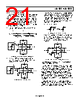
17 / 26 page  Data Sheet ADA4950-1/ADA4950-2 Rev. B | Page 17 of 26 TERMINOLOGY +IN –IN +OUT –OUT +INA +INB –INB –INA VOCM RGA 500Ω VOUT, dm RL, dm ADA4950-x RGB 250Ω RGB 250Ω RF 500Ω RF 500Ω RGA 500Ω Figure 52. Signal and Circuit Definitions Differential Voltage Differential voltage refers to the difference between two node voltages. For example, the output differential voltage (or equiv- alently, output differential node voltage) is defined as VOUT, dm = (V+OUT − V−OUT) where V+OUT and V−OUT refer to the voltages at the +OUT and −OUT output terminals with respect to a common ground reference. The input differential voltage is defined in different ways, depending upon the selected gain. For G = 1 VIN, dm = (+INA − (−INA)) where +INA and −INA refer to the voltages at the +INA and −INA input terminals with respect to a common ground reference (input terminals +INB and −INB are floating). For G = 2 VIN, dm = (+INB − (−INB)) where +INB and −INB refer to the voltages at the +INB and −INB input terminals with respect to a common ground reference (input terminals +INA and −INA are floating). For G = 3, input terminals +INA and +INB are connected together, and input terminals −INA and −INB are connected together. VIN, dm = (+INAB − (−INAB)) where +INAB and −INAB refer to the voltages at the connection of input terminals +INA and +INB and at the connection of input terminals −INA and −INB with respect to a common ground reference. Common-Mode Voltage Common-mode voltage refers to the average of two node voltages with respect to the local ground reference. The output common-mode voltage is defined as VOUT, cm = (V+OUT + V−OUT)/2 Output Balance Output balance is a measure of how close the output differential signals are to being equal in amplitude and opposite in phase. Any imbalances in amplitude or phase produce an undesired common-mode signal at the amplifier output. Output balance error is defined as the magnitude of the output common-mode voltage divided by the magnitude of the output differential mode voltage. dm OUT cm OUT V V Error Balance Output , , ∆ ∆ = |
|
|
링크 URL |
| ALLDATASHEET 가 귀하에 도움이 되셨나요? [ DONATE ] |
Alldatasheet는? | 광고문의 | 운영자에게 연락하기 | 개인정보취급방침 | 링크 투 데이터시트 | 링크교환 | 제조사별 검색 All Rights Reserved©Alldatasheet.com |
| Russian : Alldatasheetru.com | Korean : Alldatasheet.co.kr | Spanish : Alldatasheet.es | French : Alldatasheet.fr | Italian : Alldatasheetit.com Portuguese : Alldatasheetpt.com | Polish : Alldatasheet.pl | Vietnamese : Alldatasheet.vn Indian : Alldatasheet.in | Mexican : Alldatasheet.com.mx | British : Alldatasheet.co.uk | New Zealand : Alldatasheet.co.nz |
|
Family Site : ic2ic.com |
icmetro.com |
 Korean ▼
 English
 Chinese
 German
 Japanese
 Russian
 Korean
 Spanish
 French
 Italian
 Portuguese
 Polish
 Vietnamese
 Indian
 Mexican
 British
 New Zealand