|
전자부품 데이터시트 검색엔진 |
|
|
전자부품 데이터시트 검색엔진 |
|
4242-01 데이터시트(PDF) 4 Page - Peregrine Semiconductor Corp. |
|
|
|||||||||||||||||||||||||||||
4242-01 데이터시트(HTML) 4 Page - Peregrine Semiconductor Corp. |
|
|
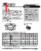
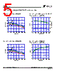
4 / 9 page  Product Specification PE4242 Page 4 of 9 ©2003-2006 Peregrine Semiconductor Corp. All rights reserved. Document No. 70-0095-03 │ UltraCMOS™ RFIC Solutions Evaluation Kit The SPDT Switch Evaluation Kit board was designed to ease customer evaluation of the PE4242 SPDT switch. The RF common port is connected through a 50 Ω transmission line to the top left SMA connector, J1. Port 1 and Port 2 are connected through 50 Ω transmission lines to the top two SMA connectors on the right side of the board, J3 and J2, respectively. A through transmission line connects SMA connectors J4 and J5. This transmission line can be used to estimate the loss of the PCB over the environmental conditions being evaluated. The board is constructed of a two metal layer FR4 material with a total thickness of 0.031”. The bottom layer provides ground for the RF transmission lines. The transmission lines were designed using a coplanar waveguide with ground plane model using a trace width of 0.0476”, trace gaps of 0.030”, dielectric thickness of 0.028”, metal thickness of 0.0021” and ε r of 4.4. J6 provides a means for controlling DC and digital inputs to the device. Starting from the lower left pin, the second pin to the right (J6-3) is connected to the device V1 or CTRL input. The fourth pin to the right (J6-7) is connected to the device V2 or CTRL /VDD input. Figure 4. Evaluation Board Layout Figure 5. Evaluation Board Schematic Peregrine Specification 101/0083 Peregrine Specification 102/0145 |
|
|
링크 URL |
| ALLDATASHEET 가 귀하에 도움이 되셨나요? [ DONATE ] |
Alldatasheet는? | 광고문의 | 운영자에게 연락하기 | 개인정보취급방침 | 링크 투 데이터시트 | 링크교환 | 제조사별 검색 All Rights Reserved©Alldatasheet.com |
| Russian : Alldatasheetru.com | Korean : Alldatasheet.co.kr | Spanish : Alldatasheet.es | French : Alldatasheet.fr | Italian : Alldatasheetit.com Portuguese : Alldatasheetpt.com | Polish : Alldatasheet.pl | Vietnamese : Alldatasheet.vn Indian : Alldatasheet.in | Mexican : Alldatasheet.com.mx | British : Alldatasheet.co.uk | New Zealand : Alldatasheet.co.nz |
|
Family Site : ic2ic.com |
icmetro.com |
 Korean ▼
 English
 Chinese
 German
 Japanese
 Russian
 Korean
 Spanish
 French
 Italian
 Portuguese
 Polish
 Vietnamese
 Indian
 Mexican
 British
 New Zealand