|
전자부품 데이터시트 검색엔진 |
|
|
전자부품 데이터시트 검색엔진 |
|
ADRF5545ABCPZN-R7 데이터시트(PDF) 2 Page - Analog Devices |
|
|
|||||||||||||||||||||||||||||
ADRF5545ABCPZN-R7 데이터시트(HTML) 2 Page - Analog Devices |
|
|
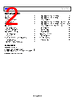
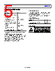
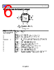
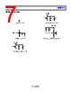
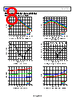
2 / 20 page  ADRF5545A Data Sheet Rev. B | Page 2 of 20 TABLE OF CONTENTS Features.............................................................................................. 1 Applications ...................................................................................... 1 Functional Block Diagram .............................................................. 1 General Description......................................................................... 1 Revision History ............................................................................... 2 Specifications .................................................................................... 3 Electrical Specifications............................................................... 3 2.6 GHz Tuned Operation .......................................................... 4 Absolute Maximum Ratings ........................................................... 5 Thermal Resistance ...................................................................... 5 ESD Caution.................................................................................. 5 Pin Configuration and Function Descriptions ............................ 6 Interface Schematics .................................................................... 7 Typical Performance Characteristics............................................. 8 Receive Operation, High Gain Mode.........................................8 Receive Operation, Low Gain Mode ....................................... 10 Transmit Operation................................................................... 12 Receive Operation, High Gain Mode with 2.6 GHz Tuning 13 Receive Operation, Low Gain Mode with 2.6 GHz Tuning. 15 Transmit Operation at with 2.6 GHz Tuning ........................ 17 Theory of Operation ...................................................................... 18 Signal Path Select........................................................................ 18 Biasing Sequence........................................................................ 18 Applications Information ............................................................. 19 2.6 GHz Operation..................................................................... 19 Outline Dimensions....................................................................... 20 Ordering Guide .......................................................................... 20 REVISION HISTORY 4/2020—Rev. A to Rev. B Changes to Theory of Operation Section.................................... 18 Changes to Applications Information Section and Figure 47...... 19 5/2019—Revision A: Initial Version |
|
|
링크 URL |
| ALLDATASHEET 가 귀하에 도움이 되셨나요? [ DONATE ] |
Alldatasheet는? | 광고문의 | 운영자에게 연락하기 | 개인정보취급방침 | 링크 투 데이터시트 | 링크교환 | 제조사별 검색 All Rights Reserved©Alldatasheet.com |
| Russian : Alldatasheetru.com | Korean : Alldatasheet.co.kr | Spanish : Alldatasheet.es | French : Alldatasheet.fr | Italian : Alldatasheetit.com Portuguese : Alldatasheetpt.com | Polish : Alldatasheet.pl | Vietnamese : Alldatasheet.vn Indian : Alldatasheet.in | Mexican : Alldatasheet.com.mx | British : Alldatasheet.co.uk | New Zealand : Alldatasheet.co.nz |
|
Family Site : ic2ic.com |
icmetro.com |
 Korean ▼
 English
 Chinese
 German
 Japanese
 Russian
 Korean
 Spanish
 French
 Italian
 Portuguese
 Polish
 Vietnamese
 Indian
 Mexican
 British
 New Zealand