|
전자부품 데이터시트 검색엔진 |
|
|
전자부품 데이터시트 검색엔진 |
|
PL135-37SC-R 데이터시트(PDF) 2 Page - Micrel Semiconductor |
|
|
|||||||||||||||||||||||||||||
PL135-37SC-R 데이터시트(HTML) 2 Page - Micrel Semiconductor |
|
|
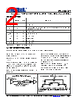
2 / 5 page  PL135-37 Low Power, 1.62V to 3. 63V, 10M Hz to 40M Hz, 1:3 O scillat or Fanout Buffer Micrel Inc. • 2180 Fortune Drive • San Jose, CA 95131 • USA • tel +1(408) 944 -0800 • fax +1(408) 474-1000 • www.micrel.com Rev 03/18/11 Page 2 PIN DESCRIPTION Name SOP-8L Type Description XIN 1 I Crystal input OE 2 I Output enable input. This pin has internal pull-up resistor. All outputs will be tri-stated when pulled low. CLK1 3 O Output clock GND 4 P Ground connection CLK2 5 O Output clock VDD 6 P Power supply CLK0 7 O Output clock XOUT 8 I Crystal output * Note: This pin includes an internal 60KΩ pull up. LAYOUT RECOMMENDATIONS The following guidelines are to assist you with a performance optimized PCB design: Signal Integrity and Termination Considerations - Keep traces short! - Trace = Inductor. With a capacitive load this equals ringing! - Long trace = Transmission Line. Without proper ter- mination this will cause reflections (looks like ringing). - Design long traces as “striplines” or “microstrips” with defined impedance. - Match trace at one side to avoid reflections bouncing back and forth. Decoupling and Power Supply Considerations - Place decoupling capacitors as close as possible to the VDD pin(s) to limit noise from the power supply - Multiple VDD pins should be decoupled separately for best performance. - Addition of a ferrite bead in series with V DD can help prevent noise from other board sources - Value of decoupling capacitor is frequency de- pendant. Typical value to use is 0.1 F. Typical CMOS termination Place Series Resistor as close as possible to CMOS output CMOS Output Buffer (Typical buffer impedance 20Ω) To CMOS Input Series Resistor Use value to match output buffer impedance to 50Ω trace. Typical value 30Ω 50Ω line Crystal Tuning Circuit Series and parallel capacitors used to fine tune the crystal load to the circuit load. CST – Series Capacitor, used to lower circuit load to match crystal load. Raises frequency offset. This can be eliminated by using a crystal with a Cload of equal or greater value than the oscillator. CPT – Parallel Capacitors, Used to raise the circuit load to match the crystal load. Lowers frequency offset. Crystal XIN 1 8 XOUT Cpt Cpt Cst |
|
|
링크 URL |
| ALLDATASHEET 가 귀하에 도움이 되셨나요? [ DONATE ] |
Alldatasheet는? | 광고문의 | 운영자에게 연락하기 | 개인정보취급방침 | 링크 투 데이터시트 | 링크교환 | 제조사별 검색 All Rights Reserved©Alldatasheet.com |
| Russian : Alldatasheetru.com | Korean : Alldatasheet.co.kr | Spanish : Alldatasheet.es | French : Alldatasheet.fr | Italian : Alldatasheetit.com Portuguese : Alldatasheetpt.com | Polish : Alldatasheet.pl | Vietnamese : Alldatasheet.vn Indian : Alldatasheet.in | Mexican : Alldatasheet.com.mx | British : Alldatasheet.co.uk | New Zealand : Alldatasheet.co.nz |
|
Family Site : ic2ic.com |
icmetro.com |
 Korean ▼
 English
 Chinese
 German
 Japanese
 Russian
 Korean
 Spanish
 French
 Italian
 Portuguese
 Polish
 Vietnamese
 Indian
 Mexican
 British
 New Zealand