|
전자부품 데이터시트 검색엔진 |
|
|
전자부품 데이터시트 검색엔진 |
|
AM261...ZEJQ1 데이터시트(PDF) 72 Page - Texas Instruments |
|
|
|||||||||||||||||||||||||||||
AM261...ZEJQ1 데이터시트(HTML) 72 Page - Texas Instruments |
|
|
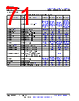
72 / 218 page  Table 5-44. Power Supply Signal Descriptions (continued) Signal Name [1] Pin Type [2] Description [3] ZCZ PIN [4] ZFG PIN [4] ZEJ PIN [4] ZNC PIN [4] VSS GND Ground A1, A18, E10, E12, E13, E14, E5, E6, E7, E8, F10, F12, F13, F14, F5, F6, F7, F8, G10, G11, G12, G7, G8, G9, H10, H11, H12, H13, H14, H5, H6, H7, H8, H9, J10, J11, J12, J13, J14, J5, J6, J7, J8, J9, K10, K11, K12, K7, K8, K9, L10, L11, L12, L13, L14, L5, L6, L7, L8, L9, M10, M11, M12, M13, M14, M5, M6, M7, M8, M9, N10, N11, N12, N7, N8, N9, P13, P14, P5, T2, V18 A1, A20, F15, F6, G10, G11, G12, G13, G14, G7, G8, G9, H10, H11, H12, H13, H14, H7, H8, H9, J10, J11, J12, J13, J14, J7, J8, J9, K10, K11, K12, K13, K14, K7, K8, K9, L10, L11, L12, L13, L14, L7, L8, L9, M10, M11, M12, M13, M14, M7, M8, M9, N10, N11, N12, N13, N14, N7, N8, N9, P10, P11, P12, P13, P14, P7, P8, P9, R14, R15, R6, V2, V5, W2, Y1, Y20 A1, A16, E10, E12, E6, E8, F10, F11, F5, F6, F7, F8, F9, G10, G11, G12, G6, G7, G8, G9, H10, H11, H5, H6, H7, H8, H9, J10, J11, J12, J6, J7, J8, J9, K10, K11, K5, K6, K7, K8, K9, L10, L11, L12, L6, L7, L8, L9, M5, M7, R2, R3, R4, T1, T16 A1, A19, D16, D4, E15, E5, F10, F11, F12, F13, F14, F6, F7, F8, F9, G10, G11, G12, G13, G14, G6, G7, G8, G9, H10, H11, H12, H13, H14, H6, H7, H8, H9, J10, J11, J12, J13, J14, J6, J7, J8, J9, K10, K11, K12, K13, K14, K6, K7, K8, K9, L10, L11, L12, L13, L14, L6, L7, L8, L9, M10, M11, M12, M13, M14, M6, M7, M8, M9, N10, N11, N12, N13, N14, N6, N7, N8, N9, P10, P11, P12, P13, P14, P6, P7, P8, P9, R14, R5, R8, T4, U2, V2, V3, W1, W19 VSSA AGND Analog Ground P10, P12, P6, P8, R13, R5, V1, V16 R12, R9 M11, M9 R10, R12 (1) See Recommended Operating Conditions for more information about the core voltage for a specific device. (2) See the Layout Guidelines sections for details on connecting this pin. (3) PCB should directly route VDDS18_LDO to all of the VDDS18 pins. (4) On AM261x, the Analog LDO is connected internally to the 1.8V analog supply and therefore functions as a regular 1.8V output. 5.3.18 PRU-ICSS Table 5-45. PRU-ICSS ECAP Signal Descriptions Signal Name [1] Pin Type [2] Description [3] ZCZ PIN [4] ZFG PIN [4] ZEJ PIN [4] ZNC PIN [4] PR0_ECAP0_APWM_OUT O PRU-ICSS Enhanced Capture (ECAP) Input or ECAP Auxiliary PWM (APWM) Output D14 C16 A15 PR1_ECAP0_APWM_OUT O PRU-ICSS Enhanced Capture (ECAP) Input or ECAP Auxiliary PWM (APWM) Output D14 C16 A15 AM2612, AM2611, AM2611-Q1, AM2612-Q1 SPRSPA7C – SEPTEMBER 2024 – REVISED JULY 2025 www.ti.com 72 Submit Document Feedback Copyright © 2025 Texas Instruments Incorporated Product Folder Links: AM2612 AM2611 AM2611-Q1 AM2612-Q1 |
|
링크 URL |
| ALLDATASHEET 가 귀하에 도움이 되셨나요? [ DONATE ] |
Alldatasheet는? | 광고문의 | 운영자에게 연락하기 | 개인정보취급방침 | 링크 투 데이터시트 | 링크교환 | 제조사별 검색 All Rights Reserved©Alldatasheet.com |
| Russian : Alldatasheetru.com | Korean : Alldatasheet.co.kr | Spanish : Alldatasheet.es | French : Alldatasheet.fr | Italian : Alldatasheetit.com Portuguese : Alldatasheetpt.com | Polish : Alldatasheet.pl | Vietnamese : Alldatasheet.vn Indian : Alldatasheet.in | Mexican : Alldatasheet.com.mx | British : Alldatasheet.co.uk | New Zealand : Alldatasheet.co.nz |
|
Family Site : ic2ic.com |
icmetro.com |
 Korean ▼
 English
 Chinese
 German
 Japanese
 Russian
 Korean
 Spanish
 French
 Italian
 Portuguese
 Polish
 Vietnamese
 Indian
 Mexican
 British
 New Zealand