|
전자부품 데이터시트 검색엔진 |
|
|
전자부품 데이터시트 검색엔진 |
|
M95020-RBN6G 데이터시트(PDF) 7 Page - STMicroelectronics |
|
|
|||||||||||||||||||||||||||||
M95020-RBN6G 데이터시트(HTML) 7 Page - STMicroelectronics |
|
|
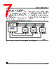
7 / 37 page  7/37 M95040, M95020, M95010 CONNECTING TO THE SPI BUS These devices are fully compatible with the SPI protocol. All instructions, addresses and input data bytes are shifted in to the device, most significant bit first. The Serial Data Input (D) is sampled on the first rising edge of the Serial Clock (C) after Chip Select (S) goes Low. All output data bytes are shifted out of the device, most significant bit first. The Serial Data Output (Q) is latched on the first falling edge of the Serial Clock (C) after the instruction (such as the Read from Memory Array and Read Status Register in- structions) have been clocked into the device. Figure 4. shows three devices, connected to an MCU, on a SPI bus. Only one device is selected at a time, so only one device drives the Serial Data Output (Q) line at a time, all the others being high impedance. Figure 4. Bus Master and Memory Devices on the SPI Bus Note: The Write Protect (W) and Hold (HOLD) signals should be driven, High or Low as appropriate. AI03746D Bus Master (ST6, ST7, ST9, ST10, Others) SPI Memory Device SDO SDI SCK CQD S SPI Memory Device CQD S SPI Memory Device CQD S CS3 CS2 CS1 SPI Interface with (CPOL, CPHA) = (0, 0) or (1, 1) W HOLD W HOLD W HOLD |
|
링크 URL |
| ALLDATASHEET 가 귀하에 도움이 되셨나요? [ DONATE ] |
Alldatasheet는? | 광고문의 | 운영자에게 연락하기 | 개인정보취급방침 | 링크 투 데이터시트 | 링크교환 | 제조사별 검색 All Rights Reserved©Alldatasheet.com |
| Russian : Alldatasheetru.com | Korean : Alldatasheet.co.kr | Spanish : Alldatasheet.es | French : Alldatasheet.fr | Italian : Alldatasheetit.com Portuguese : Alldatasheetpt.com | Polish : Alldatasheet.pl | Vietnamese : Alldatasheet.vn Indian : Alldatasheet.in | Mexican : Alldatasheet.com.mx | British : Alldatasheet.co.uk | New Zealand : Alldatasheet.co.nz |
|
Family Site : ic2ic.com |
icmetro.com |
 Korean ▼
 English
 Chinese
 German
 Japanese
 Russian
 Korean
 Spanish
 French
 Italian
 Portuguese
 Polish
 Vietnamese
 Indian
 Mexican
 British
 New Zealand