|
전자부품 데이터시트 검색엔진 |
|
|
전자부품 데이터시트 검색엔진 |
|
H8SX/1663 데이터시트(PDF) 783 Page - Renesas Technology Corp |
|
|
|||||||||||||||||||||||||||||
H8SX/1663 데이터시트(HTML) 783 Page - Renesas Technology Corp |
|
|
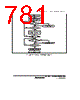
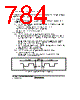
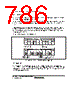
783 / 1158 page  Section 15 Serial Communication Interface (SCI, IrDA, CRC) Rev.1.00 Jun. 07, 2006 Page 731 of 1102 REJ09B0294-0100 Initialization Read data from RDR and clear RDRF flag in SSR to 0 Clear RE bit in SCR to 0 Start reception Start Error processing No No No Yes Yes ORER = 0 and PER = 0? RDRF = 1? All data received? Yes Figure 15.33 Sample Reception Flowchart 15.7.8 Clock Output Control Clock output can be fixed using the CKE1 and CKE0 bits in SCR when the GM bit in SMR is set to 1. Specifically, the minimum width of a clock pulse can be specified. Figure 15.34 shows an example of clock output fixing timing when the CKE0 bit is controlled with GM = 1 and CKE1 = 0. Given pulse width SCK CKE0 Given pulse width Figure 15.34 Clock Output Fixing Timing |
|
링크 URL |
| ALLDATASHEET 가 귀하에 도움이 되셨나요? [ DONATE ] |
Alldatasheet는? | 광고문의 | 운영자에게 연락하기 | 개인정보취급방침 | 링크 투 데이터시트 | 링크교환 | 제조사별 검색 All Rights Reserved©Alldatasheet.com |
| Russian : Alldatasheetru.com | Korean : Alldatasheet.co.kr | Spanish : Alldatasheet.es | French : Alldatasheet.fr | Italian : Alldatasheetit.com Portuguese : Alldatasheetpt.com | Polish : Alldatasheet.pl | Vietnamese : Alldatasheet.vn Indian : Alldatasheet.in | Mexican : Alldatasheet.com.mx | British : Alldatasheet.co.uk | New Zealand : Alldatasheet.co.nz |
|
Family Site : ic2ic.com |
icmetro.com |
 Korean ▼
 English
 Chinese
 German
 Japanese
 Russian
 Korean
 Spanish
 French
 Italian
 Portuguese
 Polish
 Vietnamese
 Indian
 Mexican
 British
 New Zealand