|
전자부품 데이터시트 검색엔진 |
|
|
전자부품 데이터시트 검색엔진 |
|
CM6800AGIS 데이터시트(PDF) 14 Page - Champion Microelectronic Corp. |
|
|
|||||||||||||||||||||||||||||
CM6800AGIS 데이터시트(HTML) 14 Page - Champion Microelectronic Corp. |
|
|
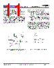
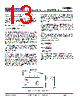
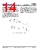
14 / 18 page  CM6800A LOW START-UP CURRENT PFC/PWM CONTROLLER COMBO 2009/08/10 Rev. 1.6 Champion Microelectronic Corporation Page 14 Leading/Trailing Modulation Conventional Pulse Width Modulation (PWM) techniques employ trailing edge modulation in which the switch will turn on right after the trailing edge of the system clock. The error amplifier output is then compared with the modulating ramp up. The effective duty cycle of the trailing edge modulation is determined during the ON time of the switch. Figure 4 shows a typical trailing edge control scheme. In case of leading edge modulation, the switch is turned OFF right at the leading edge of the system clock. When the modulating ramp reaches the level of the error amplifier output voltage, the switch will be turned ON. The effective duty-cycle of the leading edge modulation is determined during OFF time of the switch. Figure 5 shows a leading edge control scheme. One of the advantages of this control technique is that it required only one system clock. Switch 1(SW1) turns off and switch 2 (SW2) turns on at the same instant to minimize the momentary “no-load” period, thus lowering ripple voltage generated by the switching action. With such synchronized switching, the ripple voltage of the first stage is reduced. Calculation and evaluation have shown that the 120Hz component of the PFC’s output ripple voltage can be reduced by as much as 30% using this method. |
|
|
링크 URL |
| ALLDATASHEET 가 귀하에 도움이 되셨나요? [ DONATE ] |
Alldatasheet는? | 광고문의 | 운영자에게 연락하기 | 개인정보취급방침 | 링크 투 데이터시트 | 링크교환 | 제조사별 검색 All Rights Reserved©Alldatasheet.com |
| Russian : Alldatasheetru.com | Korean : Alldatasheet.co.kr | Spanish : Alldatasheet.es | French : Alldatasheet.fr | Italian : Alldatasheetit.com Portuguese : Alldatasheetpt.com | Polish : Alldatasheet.pl | Vietnamese : Alldatasheet.vn Indian : Alldatasheet.in | Mexican : Alldatasheet.com.mx | British : Alldatasheet.co.uk | New Zealand : Alldatasheet.co.nz |
|
Family Site : ic2ic.com |
icmetro.com |
 Korean ▼
 English
 Chinese
 German
 Japanese
 Russian
 Korean
 Spanish
 French
 Italian
 Portuguese
 Polish
 Vietnamese
 Indian
 Mexican
 British
 New Zealand