|
전자부품 데이터시트 검색엔진 |
|
|
전자부품 데이터시트 검색엔진 |
|
ATR4252-RAPW 데이터시트(PDF) 6 Page - ATMEL Corporation |
|
|
|||||||||||||||||||||||||||||
ATR4252-RAPW 데이터시트(HTML) 6 Page - ATMEL Corporation |
|
|
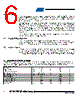
6 / 10 page  6 9154AS–AUDR–09/09 ATR4252 [Preliminary] 3.4 FM AGC The IC is equipped with an AGC capability to prevent overdriving of the amplifier in case the amplifier is operated at strong antenna signals, e.g., near transmitters. It is possible to realize an additional antenna amplifier path with integrated AGC and external RF transistor. The bandwidth of the integrated AGC circuit is 900 MHz. FM amplifier output FMC is connected to a capacitive voltage divider and the divided signal is applied to the AGC level detector at pin FMDET. This level detector input is optimized for low distortion. The rectified signal is compared against an internal reference. The threshold of the AGC can be adjusted by tuning the divider ratio of the external voltage divider. If the threshold is reached, pin FMPD opens an internal transistor, which controls the pin-diode current. By these means, the amplifier input signal is limited and therefore the FM amplifier is prevented from sig- nal overdrive. The necessary driver for the external pin diode is already incorporated in the ATR4252 IC, which reduces the BOM cost and the application size. 3.5 Supply Voltage Regulator The driving voltage for an external power transistor is provided by an integrated regulator circuit. An overvoltage protection circuit recognizes overvoltage condition and switches off the amplifier and AGC circuits in order to reduce current consumption and avoid thermal overload. 3.6 Antenna Sensor In addition, an antenna sensor has been integrated in order to recognize if the antenna is prop- erly connected to the amplifier module. If no antenna is detected, the amplifier and AGC circuits are switched off in order to signal this error via reduction of supply current consumption to the unit that provides and monitors the supply current for the antenna amplifier (e.g., the car radio). 4. Absolute Maximum Ratings Stresses beyond those listed under “Absolute Maximum Ratings” may cause permanent damage to the device. This is a stress rating only and functional operation of the device at these or any other conditions beyond those indicated in the operational sections of this specification is not implied. Exposure to absolute maximum rating conditions for extended periods may affect device reliability. Reference point is ground. Parameters Pin Symbol Min. Max. Unit Supply voltage 11 VS –0.3 +12 V Collector of FM amplifier 14 FMC 3 16 V AM LNA input terminal 23 AM LNA IN 0 2 V AM LNA output terminal 26 AM LNA OUT 7 12 V Power dissipation Ptot 1200 mW Junction temperature Tj 150 °C Ambient temperature Tamb –40 +105 °C Storage temperature Tstg –50 +150 °C ESD HBM all VHBM –2 +2 kV |
|
|
링크 URL |
| ALLDATASHEET 가 귀하에 도움이 되셨나요? [ DONATE ] |
Alldatasheet는? | 광고문의 | 운영자에게 연락하기 | 개인정보취급방침 | 링크 투 데이터시트 | 링크교환 | 제조사별 검색 All Rights Reserved©Alldatasheet.com |
| Russian : Alldatasheetru.com | Korean : Alldatasheet.co.kr | Spanish : Alldatasheet.es | French : Alldatasheet.fr | Italian : Alldatasheetit.com Portuguese : Alldatasheetpt.com | Polish : Alldatasheet.pl | Vietnamese : Alldatasheet.vn Indian : Alldatasheet.in | Mexican : Alldatasheet.com.mx | British : Alldatasheet.co.uk | New Zealand : Alldatasheet.co.nz |
|
Family Site : ic2ic.com |
icmetro.com |
 Korean ▼
 English
 Chinese
 German
 Japanese
 Russian
 Korean
 Spanish
 French
 Italian
 Portuguese
 Polish
 Vietnamese
 Indian
 Mexican
 British
 New Zealand