|
전자부품 데이터시트 검색엔진 |
|
|
전자부품 데이터시트 검색엔진 |
|
HT7939 데이터시트(PDF) 5 Page - Holtek Semiconductor Inc |
|
|
|||||||||||||||||||||||||||||
HT7939 데이터시트(HTML) 5 Page - Holtek Semiconductor Inc |
|
|
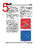
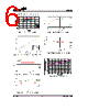
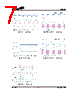
5 / 13 page  HT7939 Rev 1.10 5 November 3, 2009 · Schottky Diode Selection The output rectifier diode conducts during the internal MOSFET is turn off. The average and peak current rating must be greater than the maximum output cur- rent and peak inductor current. The reverse break- down voltage must be greater than the maximum output voltage. It is recommended to use a schottky diode with low forward voltage to minimize the power dissipation and therefore to maximize the efficiency of the converter. A 1N5819 type diode is recommended for HT7939 applications. · LED Current Selection The LED current is controlled by the current sense feedback resistor Rfb, The current sense feedback ref- erence voltage is 200mV. In order to have accurate LED currents, precision resistors are the preferred type with a 1% tolerance. The LED current can be cal- culated from the following formula. Where ILED is the total output LED current, VFB=feed- back voltage, Rfb=current sense resistor. · Digital and Analog Dimming Control The LED illumination level can be controlled using both digital and analog methods. The digital method uses a PWM signal applied to the EN pin. This is shown in figure 14. The average LED current increases proportionally with the PWM signal duty cycle. A 0% duty cycle corresponds to zero LED current. A 100% duty cycle corresponds to full LED current. The PWM signal frequency should be set be- low 1kHz due to the delay time of device startup. There are two methods of analog LED brightness con- trol. The first method uses a DC voltage to control the feedback voltage. If the DC voltage range is from 0V to 3.3V, the selection of resistors control the LED cur- rent from 20mA to 0mA as shown in figure15. The other way is to use a filtered PWM signal, as shown in figure16. The filtered PWM signal application acts in the same way as the DC voltage dimming control. Layout Considerations Circuit board layout is a very important consideration for switching regulators if they are to function properly. Poor circuit layout may result in related noise problems. In order to minimize EMI and switching noise, please fol- low the guidelines below: · All tracks should be as wide as possible. · The input and output capacitors, C1 and C2, should be placed close to the VIN, VO and GND pins. · The Schottky diode, D1, and inductor, L, must be placed close to the SW pin. · Feedback resistor, Rfb, must be placed close to the FB and GND pins. · A full ground plane is always helpful for better EMI performance. A recommended PCB layout with component locations is shown below. f b R f b R F B V L E D I 2 0 0 m V = = Top Layer Bottom Layer |
|
|
링크 URL |
| ALLDATASHEET 가 귀하에 도움이 되셨나요? [ DONATE ] |
Alldatasheet는? | 광고문의 | 운영자에게 연락하기 | 개인정보취급방침 | 링크 투 데이터시트 | 링크교환 | 제조사별 검색 All Rights Reserved©Alldatasheet.com |
| Russian : Alldatasheetru.com | Korean : Alldatasheet.co.kr | Spanish : Alldatasheet.es | French : Alldatasheet.fr | Italian : Alldatasheetit.com Portuguese : Alldatasheetpt.com | Polish : Alldatasheet.pl | Vietnamese : Alldatasheet.vn Indian : Alldatasheet.in | Mexican : Alldatasheet.com.mx | British : Alldatasheet.co.uk | New Zealand : Alldatasheet.co.nz |
|
Family Site : ic2ic.com |
icmetro.com |
 Korean ▼
 English
 Chinese
 German
 Japanese
 Russian
 Korean
 Spanish
 French
 Italian
 Portuguese
 Polish
 Vietnamese
 Indian
 Mexican
 British
 New Zealand