|
전자부품 데이터시트 검색엔진 |
|
|
전자부품 데이터시트 검색엔진 |
|
WM2614 데이터시트(PDF) 8 Page - Wolfson Microelectronics plc |
|
|
|||||||||||||||||||||||||||||
WM2614 데이터시트(HTML) 8 Page - Wolfson Microelectronics plc |
|
|
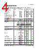
8 / 10 page  WM2614 Production Data Rev 1.0 WOLFSON MICROELECTRONICS LTD Production Data Rev 1.0 June 1999 8 DEVICE DESCRIPTION GENERAL FUNCTION The device uses a resistor string network buffered with an op amp to convert 12-bit digital data to analogue voltage levels (see Block Diagram). The output voltage is determined by the reference input voltage and the input code according to the following relationship: Output voltage = ( ) 4096 CODE V 2 REF INPUT OUTPUT 1111 1111 1111 ( ) 4096 4095 V 2 REF : : 1000 0000 0001 ( ) 4096 2049 V 2 REF 1000 0000 0000 ( ) REF REF V 4096 2048 V 2 = 0111 1111 1111 ( ) 4096 2047 V 2 REF : : 0000 0000 0001 ( ) 4096 1 V 2 REF 0000 0000 0000 0V Table 1 Binary Code Table (0V to 2VREFIN Output), Gain = 2 POWER ON RESET An internal power-on-reset circuit resets the DAC register to all 0s on power-up. BUFFER AMPLIFIER The output buffer has a near rail-to-rail output with short circuit protection and can reliably drive a 2k Ω load with a 100pF load capacitance. EXTERNAL REFERENCE The reference voltage input is buffered which makes the DAC input resistance independent of code. The REFIN pin has an input resistance of 10M Ω and an input capacitance of typically 5pF. The reference voltage determines the DAC full-scale output. HARDWARE CONFIGURATION OPTIONS The device has two configuration options that are controlled by device pins. DEVICE POWER DOWN The device can be powered-down by pulling pin NPD (Pin 2) high. This powers down all DACs overriding their individual power down settings. This will reduce power consumption to typically 10nA. When the power down function is released the device reverts to the DAC code set prior to power down. SIMULTANEOUS DAC UPDATE The NLDAC pin (Pin 3) can be held high to prevent serial word writes from updating the DAC latches. By writing new values to multiple DACs then pulling NLDAC low, all new DAC codes are loaded into the DAC latches simultaneously. |
|
|
링크 URL |
| ALLDATASHEET 가 귀하에 도움이 되셨나요? [ DONATE ] |
Alldatasheet는? | 광고문의 | 운영자에게 연락하기 | 개인정보취급방침 | 링크 투 데이터시트 | 링크교환 | 제조사별 검색 All Rights Reserved©Alldatasheet.com |
| Russian : Alldatasheetru.com | Korean : Alldatasheet.co.kr | Spanish : Alldatasheet.es | French : Alldatasheet.fr | Italian : Alldatasheetit.com Portuguese : Alldatasheetpt.com | Polish : Alldatasheet.pl | Vietnamese : Alldatasheet.vn Indian : Alldatasheet.in | Mexican : Alldatasheet.com.mx | British : Alldatasheet.co.uk | New Zealand : Alldatasheet.co.nz |
|
Family Site : ic2ic.com |
icmetro.com |
 Korean ▼
 English
 Chinese
 German
 Japanese
 Russian
 Korean
 Spanish
 French
 Italian
 Portuguese
 Polish
 Vietnamese
 Indian
 Mexican
 British
 New Zealand