|
전자부품 데이터시트 검색엔진 |
|
|
전자부품 데이터시트 검색엔진 |
|
M95320-R 데이터시트(PDF) 9 Page - STMicroelectronics |
|
|
|||||||||||||||||||||||||||||
M95320-R 데이터시트(HTML) 9 Page - STMicroelectronics |
|
|
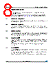
9 / 44 page  M95320, M95320-W, M95320-R Signal description Doc ID 5711 Rev 12 9/44 2.6 Write Protect (W) The main purpose of this input signal is to freeze the size of the area of memory that is protected against Write instructions (as specified by the values in the BP1 and BP0 bits of the Status Register). This pin must be driven either high or low, and must be stable during all write operations. 2.7 VSS ground VSS is the reference for the VCC supply voltage. 2.8 VCC supply voltage Refer to Section 4.1: Supply voltage (VCC) on page 12. |
|
링크 URL |
| ALLDATASHEET 가 귀하에 도움이 되셨나요? [ DONATE ] |
Alldatasheet는? | 광고문의 | 운영자에게 연락하기 | 개인정보취급방침 | 링크 투 데이터시트 | 링크교환 | 제조사별 검색 All Rights Reserved©Alldatasheet.com |
| Russian : Alldatasheetru.com | Korean : Alldatasheet.co.kr | Spanish : Alldatasheet.es | French : Alldatasheet.fr | Italian : Alldatasheetit.com Portuguese : Alldatasheetpt.com | Polish : Alldatasheet.pl | Vietnamese : Alldatasheet.vn Indian : Alldatasheet.in | Mexican : Alldatasheet.com.mx | British : Alldatasheet.co.uk | New Zealand : Alldatasheet.co.nz |
|
Family Site : ic2ic.com |
icmetro.com |
 Korean ▼
 English
 Chinese
 German
 Japanese
 Russian
 Korean
 Spanish
 French
 Italian
 Portuguese
 Polish
 Vietnamese
 Indian
 Mexican
 British
 New Zealand