|
전자부품 데이터시트 검색엔진 |
|
|
전자부품 데이터시트 검색엔진 |
|
MIC2174 데이터시트(PDF) 13 Page - Micrel Semiconductor |
|
|
|||||||||||||||||||||||||||||
MIC2174 데이터시트(HTML) 13 Page - Micrel Semiconductor |
|
|
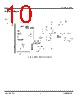
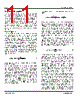
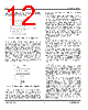
13 / 27 page  Micrel, Inc. MIC2174/MIC2174C September 2010 13 M9999-091310-C The circuit in Figure 4 illustrates the MIC2174/MIC2174C current limiting circuit. MOSFET Gate Drive The MIC2174/MIC2174C high-side drive circuit is designed to switch an N-Channel MOSFET. The block diagram of Figure 1 shows a bootstrap circuit, consisting of D1 (a Schottky diode is recommended) and CBST. This circuit supplies energy to the high-side drive circuit. Capacitor CBST is charged, while the low-side MOSFET is on, and the voltage on the LX pin is approximately 0V. When the high-side MOSFET driver is turned on, energy from CBST is used to turn the MOSFET on. As the high- side MOSFET turns on, the voltage on the LX pin increases to approximately VHSD. Diode D1 is reversed biased and CBST floats high while continuing to keep the high-side MOSFET on. The bias current of the high-side driver is less than 10mA so a 0.1μF to 1μF is sufficient to hold the gate voltage with minimal droop for the power stroke (high-side switching) cycle, i.e. ΔBST = 10mA x 3.33μs/0.1μF = 333mV. When the low-side MOSFET is turned back on, CBST is recharged through D1. A small resistor RG, which is in series with CBST, can be used to slow down the turn-on time of the high-side N-channel MOSFET. Figure 4. MIC2174/MIC2174C Current Limiting Circuit Using the typical VCL value of 130mV, the current limit value is roughly estimated as: DS(ON) CL R 130mV I ≈ The drive voltage is derived from the supply voltage VIN. The nominal low-side gate drive voltage is VIN and the nominal high-side gate drive voltage is approximately VIN – VDIODE, where VDIODE is the voltage drop across D1. An approximate 30ns delay between the high-side and low- side driver transitions is used to prevent current from simultaneously flowing unimpeded through both MOSFETs. For designs where the current ripple is significant compared to the load current IOUT, or for low duty cycle operation, calculating the current limit ICL should take into account that one is sensing the peak inductor current and that there is a blanking delay of approximately 150ns. 2 ΔI L t V R 130mV I L(pp) DLY OUT DS(ON) CL − × + = (3) L f D) (1 V ΔI SW OUT L(pp) × − × = (4) where: VOUT = The output voltage tDLY = Current limit blanking time, 150ns typical ΔIL(pp) = Inductor current ripple peak-to-peak value D = Duty Cycle fSW = Switching frequency The MOSFET RDS(ON) varies 30 to 40% with temperature. Therefore, it is recommended to add 50% margin to ICL in the above equation to avoid false current limiting due to an increased MOSFET junction temperature rise. It is also recommended to connect the LX pin directly to the drain of the low-side MOSFET to accurately sense the MOSFETs RDS(ON). |
|
|
링크 URL |
| ALLDATASHEET 가 귀하에 도움이 되셨나요? [ DONATE ] |
Alldatasheet는? | 광고문의 | 운영자에게 연락하기 | 개인정보취급방침 | 링크 투 데이터시트 | 링크교환 | 제조사별 검색 All Rights Reserved©Alldatasheet.com |
| Russian : Alldatasheetru.com | Korean : Alldatasheet.co.kr | Spanish : Alldatasheet.es | French : Alldatasheet.fr | Italian : Alldatasheetit.com Portuguese : Alldatasheetpt.com | Polish : Alldatasheet.pl | Vietnamese : Alldatasheet.vn Indian : Alldatasheet.in | Mexican : Alldatasheet.com.mx | British : Alldatasheet.co.uk | New Zealand : Alldatasheet.co.nz |
|
Family Site : ic2ic.com |
icmetro.com |
 Korean ▼
 English
 Chinese
 German
 Japanese
 Russian
 Korean
 Spanish
 French
 Italian
 Portuguese
 Polish
 Vietnamese
 Indian
 Mexican
 British
 New Zealand