|
전자부품 데이터시트 검색엔진 |
|
|
전자부품 데이터시트 검색엔진 |
|
MT-059 데이터시트(PDF) 11 Page - Analog Devices |
|
|
|||||||||||||||||||||||||||||
MT-059 데이터시트(HTML) 11 Page - Analog Devices |
|
|
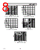
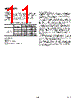
11 / 13 page  REV. D AD8072/AD8073 –10– Crosstalk Crosstalk between internal amplifiers may vary depending on which amplifier is being driven and how many amplifiers are being driven. This variation typically stems from pin location on the package and the internal layout of the IC itself. Table I illustrates the typical crosstalk results for a combination of conditions. Table I. AD8073JR Crosstalk Table (dB) Receive Amplifier AD8073JR 12 3 1 X –60 –56 Drive 2 –60 X –60 Amplifier 3 –54 –60 X All Hostile –53 –55 –54 CONDITIONS VS = ±5 V RF = 1 k Ω, R L = 150 Ω AV = 2 VOUT = 2 V p-p on Drive Amplifier Layout Considerations The specified high speed performance of the AD8072 and AD8073 require careful attention to board layout and compo- nent selection. Proper RF design techniques and low parasitic component selection are mandatory. The PCB should have a ground plane covering all unused portions of the component side of the board to provide a low impedance ground path. The ground plane should be removed from the area near the input pins to reduce stray capacitance. Chip capacitors should be used for supply bypassing. One end of the capacitor should be connected to the ground plane and the other within 1/8 inches of each power pin. An additional large (4.7 µF–10 µF) tantalum electrolytic capacitor should be connected in parallel, but not necessarily as close to the supply pins, to provide current for fast large-signal changes at the device’s output. The feedback resistor should be located close to the inverting input pin in order to keep the stray capacitance at this node to a minimum. Capacitance variations of less than 1 pF at the invert- ing input will affect high speed performance. Stripline design techniques should be used for long signal traces (greater than approximately 1 inch). These should be designed with a characteristic impedance of 50 Ω or 75 Ω and be properly terminated at each end. |
|
|
링크 URL |
| ALLDATASHEET 가 귀하에 도움이 되셨나요? [ DONATE ] |
Alldatasheet는? | 광고문의 | 운영자에게 연락하기 | 개인정보취급방침 | 링크 투 데이터시트 | 링크교환 | 제조사별 검색 All Rights Reserved©Alldatasheet.com |
| Russian : Alldatasheetru.com | Korean : Alldatasheet.co.kr | Spanish : Alldatasheet.es | French : Alldatasheet.fr | Italian : Alldatasheetit.com Portuguese : Alldatasheetpt.com | Polish : Alldatasheet.pl | Vietnamese : Alldatasheet.vn Indian : Alldatasheet.in | Mexican : Alldatasheet.com.mx | British : Alldatasheet.co.uk | New Zealand : Alldatasheet.co.nz |
|
Family Site : ic2ic.com |
icmetro.com |
 Korean ▼
 English
 Chinese
 German
 Japanese
 Russian
 Korean
 Spanish
 French
 Italian
 Portuguese
 Polish
 Vietnamese
 Indian
 Mexican
 British
 New Zealand