|
전자부품 데이터시트 검색엔진 |
|
|
전자부품 데이터시트 검색엔진 |
|
3D7702Z-O2 데이터시트(PDF) 3 Page - Data Delay Devices, Inc. |
|
|
|||||||||||||||||||||||||||||
3D7702Z-O2 데이터시트(HTML) 3 Page - Data Delay Devices, Inc. |
|
|
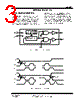
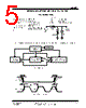
3 / 5 page  3D7702 APPLICATION NOTES OPERATIONAL DESCRIPTION The 3D7702 delay line oscillator architecture is shown in Figure 1. The internal delay line is composed of a number of delay cells connected in series and is compensated for thermal and supply voltage variations. A low-going edge on the EN input starts the oscillator, with the O2 output responding immediately. The O1 output is delayed by ½ cycle. The response of the output when the oscillator is disabled depends on the status of O2 when the EN signal goes high, as shown in Figure 2. If O2 is low, it will remain low, and the final pulse on O1 will be ½ of the period. If O2 is high, it will go low as soon as EN goes high, and the final pulse on both outputs will have a width smaller than ½ the period. Temp & Vdd Compensation Figure 1: 3D7702 Functional Diagram Delay Line EN VDD GND O1 O2 EN O1 O2 Figure 2: 3D7702 Timing Diagrams EN O1 O2 5ns typ 5ns typ 5ns typ Doc #06024 DATA DELAY DEVICES, INC. 3 12/5/2006 3 Mt. Prospect Ave. Clifton, NJ 07013 |
|
|
링크 URL |
| ALLDATASHEET 가 귀하에 도움이 되셨나요? [ DONATE ] |
Alldatasheet는? | 광고문의 | 운영자에게 연락하기 | 개인정보취급방침 | 링크 투 데이터시트 | 링크교환 | 제조사별 검색 All Rights Reserved©Alldatasheet.com |
| Russian : Alldatasheetru.com | Korean : Alldatasheet.co.kr | Spanish : Alldatasheet.es | French : Alldatasheet.fr | Italian : Alldatasheetit.com Portuguese : Alldatasheetpt.com | Polish : Alldatasheet.pl | Vietnamese : Alldatasheet.vn Indian : Alldatasheet.in | Mexican : Alldatasheet.com.mx | British : Alldatasheet.co.uk | New Zealand : Alldatasheet.co.nz |
|
Family Site : ic2ic.com |
icmetro.com |
 Korean ▼
 English
 Chinese
 German
 Japanese
 Russian
 Korean
 Spanish
 French
 Italian
 Portuguese
 Polish
 Vietnamese
 Indian
 Mexican
 British
 New Zealand