|
전자부품 데이터시트 검색엔진 |
|
|
전자부품 데이터시트 검색엔진 |
|
IDT7133LA55F 데이터시트(PDF) 11 Page - Integrated Device Technology |
|
|
|||||||||||||||||||||||||||||
IDT7133LA55F 데이터시트(HTML) 11 Page - Integrated Device Technology |
|
|
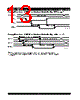
11 / 16 page  6.42 IDT7133SA/LA, IDT7143SA/LA High-Speed 2K x 16 Dual-Port RAM Military, Industrial and Commercial Temperature Ranges 11 NOTES: 1. R/ W or CE must be HIGH during all address transitions. 2. A write occurs during the overlap (tEW or tWP) of a CE = VIL and a R/W = VIL. 3. tWR is measured from the earlier of CE or R/W going HIGH to the end of the write cycle. 4. During this period, the I/O pins are in the output state, and input signals must not be applied. 5. If the CE LOW transition occurs simultaneously with or after the R/W LOW transition, the outputs remain in the High-impedance state. 6. Timing depends on which enable signal ( CE or R/W) is asserted last. 7. Timing depends on which enable signal is de-asserted first, CE or OE. 8. If OE is LOW during a R/W controlled write cycle, the write pulse width must be the larger of tWP or (tWZ + tDW) to allow the I/O drivers to turn off and data to be placed on the bus for the required tDW. If OE is HIGH during an R/W controlled write cycle, this requirement does not apply and the write pulse can be as short as the specified tWP. 9. R/ W for either upper or lower byte. Write Cycle No. 2 (CE Controlled Timing)(1,5) Timing Waveform of Write Cycle No. 1 (R/W Controlled Timing)(1,5,8) CE 2746 drw 09 tAW tAS tWR tDW DATAIN ADDRESS tWC R/ W tWP tDH DATAOUT tWZ (7) (4) (2) tOW OE (9) tLZ (7) tHZ (6) (3) (4) (7) tHZ CE 2746 drw 10 tAW tAS tWR tDW DATAIN ADDRESS tWC R/ W tEW tDH (9) (6) (2) |
|
|
링크 URL |
| ALLDATASHEET 가 귀하에 도움이 되셨나요? [ DONATE ] |
Alldatasheet는? | 광고문의 | 운영자에게 연락하기 | 개인정보취급방침 | 링크 투 데이터시트 | 링크교환 | 제조사별 검색 All Rights Reserved©Alldatasheet.com |
| Russian : Alldatasheetru.com | Korean : Alldatasheet.co.kr | Spanish : Alldatasheet.es | French : Alldatasheet.fr | Italian : Alldatasheetit.com Portuguese : Alldatasheetpt.com | Polish : Alldatasheet.pl | Vietnamese : Alldatasheet.vn Indian : Alldatasheet.in | Mexican : Alldatasheet.com.mx | British : Alldatasheet.co.uk | New Zealand : Alldatasheet.co.nz |
|
Family Site : ic2ic.com |
icmetro.com |
 Korean ▼
 English
 Chinese
 German
 Japanese
 Russian
 Korean
 Spanish
 French
 Italian
 Portuguese
 Polish
 Vietnamese
 Indian
 Mexican
 British
 New Zealand