|
전자부품 데이터시트 검색엔진 |
|
|
전자부품 데이터시트 검색엔진 |
|
9DBU0741 데이터시트(PDF) 3 Page - Integrated Circuit Systems |
|
|
|||||||||||||||||||||||||||||
9DBU0741 데이터시트(HTML) 3 Page - Integrated Circuit Systems |
|
|
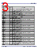
3 / 17 page  REVISION C 04/22/15 3 7 O/P 1.5V PCIE GEN1-2-3 FAN-OUT BUFFER W/ZO=100OHMS 9DBU0741 DATASHEET Pin Descriptions PIN # PIN NAME PIN TYPE DESCRIPTION 1 vSADR_tri LATCHE D IN Tri-level latch to select SMBus Address. See SMBus Address Selection Table. 2vOE6# IN Active low input for enabling DIF pair 6. This pin has an internal pull-down. 1 =disable outputs, 0 = enable outputs 3 DIF6 OUT Differential true clock output 4 DIF6# OUT Differential Complementary clock output 5 VDDR1.5 PWR 1.5V power for differential input clock (receiver). This VDD should be treated as an Analog power rail and filtered appropriately. 6 CLK_IN IN True Input for differential reference clock. 7 CLK_IN# IN Complementary Input for differential reference clock. 8 GNDDIG GND Ground pin for digital circuitry 9 SCLK_3.3 IN Clock pin of SMBus circuitry, 3.3V tolerant. 10 SDATA_3.3 I/O Data pin for SMBus circuitry, 3.3V tolerant. 11 VDDDIG1.5 PWR 1.5V digital power (dirty power) 12 VDDIO PWR Power supply for differential outputs 13 vOE0# IN Active low input for enabling DIF pair 0. This pin has an internal pull-down. 1 =disable outputs, 0 = enable outputs 14 DIF0 OUT Differential true clock output 15 DIF0# OUT Differential Complementary clock output 16 VDD1.5 PWR Power supply, nominally 1.5V 17 VDDIO PWR Power supply for differential outputs 18 DIF1 OUT Differential true clock output 19 DIF1# OUT Differential Complementary clock output 20 NC N/A No Connection. 21 vOE1# IN Active low input for enabling DIF pair 1. This pin has an internal pull-down. 1 =disable outputs, 0 = enable outputs 22 DIF2 OUT Differential true clock output 23 DIF2# OUT Differential Complementary clock output 24 vOE2# IN Active low input for enabling DIF pair 2. This pin has an internal pull-down. 1 =disable outputs, 0 = enable outputs 25 VDDA1.5 PWR 1.5V power for the PLL core. 26 VDDIO PWR Power supply for differential outputs 27 DIF3 OUT Differential true clock output 28 DIF3# OUT Differential Complementary clock output 29 vOE3# IN Active low input for enabling DIF pair 3. This pin has an internal pull-down. 1 =disable outputs, 0 = enable outputs 30 NC N/A No Connection. 31 VDD1.5 PWR Power supply, nominally 1.5V 32 VDDIO PWR Power supply for differential outputs 33 DIF4 OUT Differential true clock output 34 DIF4# OUT Differential Complementary clock output 35 vOE4# IN Active low input for enabling DIF pair 4. This pin has an internal pull-down. 1 =disable outputs, 0 = enable outputs 36 DIF5 OUT Differential true clock output 37 DIF5# OUT Differential Complementary clock output 38 vOE5# IN Active low input for enabling DIF pair 5. This pin has an internal pull-down. 1 =disable outputs, 0 = enable outputs 39 VDDIO PWR Power supply for differential outputs 40 ^CKPWRGD_PD# IN Input notifies device to sample latched inputs and start up on first high assertion. Low enters Power Down Mode, subsequent high assertions exit Power Down Mode. This pin has internal pull-up resistor. 41 ePAD GND Connect paddle to ground. |
|
|
링크 URL |
| ALLDATASHEET 가 귀하에 도움이 되셨나요? [ DONATE ] |
Alldatasheet는? | 광고문의 | 운영자에게 연락하기 | 개인정보취급방침 | 링크 투 데이터시트 | 링크교환 | 제조사별 검색 All Rights Reserved©Alldatasheet.com |
| Russian : Alldatasheetru.com | Korean : Alldatasheet.co.kr | Spanish : Alldatasheet.es | French : Alldatasheet.fr | Italian : Alldatasheetit.com Portuguese : Alldatasheetpt.com | Polish : Alldatasheet.pl | Vietnamese : Alldatasheet.vn Indian : Alldatasheet.in | Mexican : Alldatasheet.com.mx | British : Alldatasheet.co.uk | New Zealand : Alldatasheet.co.nz |
|
Family Site : ic2ic.com |
icmetro.com |
 Korean ▼
 English
 Chinese
 German
 Japanese
 Russian
 Korean
 Spanish
 French
 Italian
 Portuguese
 Polish
 Vietnamese
 Indian
 Mexican
 British
 New Zealand