|
전자부품 데이터시트 검색엔진 |
|
|
전자부품 데이터시트 검색엔진 |
|
SN74LVC2G53 데이터시트(PDF) 2 Page - Texas Instruments |
|
|
|||||||||||||||||||||||||||||
SN74LVC2G53 데이터시트(HTML) 2 Page - Texas Instruments |
|
|
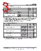
2 / 22 page  COM Y Y2 A INH Y1 COM 5 2 7 6 1 SW SW NOTE A: For simplicity, the test conditions shown in Figures 1 through 4 and 6 through 10 are for the demultiplexer configuration. Signals can be passed from COM to Y1 (Y2) or from Y1 (Y2) to COM. SN74LVC2G53 SCES324N – JULY 2001 – REVISED JANUAY 2014 www.ti.com These devices have limited built-in ESD protection. The leads should be shorted together or the device placed in conductive foam during storage or handling to prevent electrostatic damage to the MOS gates. Function Table CONTROL ON INPUTS CHANNEL INH A L L Y1 L H Y2 H X None Logic Diagram (Positive Logic) Simplified Schematic, Each Switch (SW) 2 Submit Documentation Feedback Copyright © 2001–2014, Texas Instruments Incorporated Product Folder Links :SN74LVC2G53 |
|
|
링크 URL |
| ALLDATASHEET 가 귀하에 도움이 되셨나요? [ DONATE ] |
Alldatasheet는? | 광고문의 | 운영자에게 연락하기 | 개인정보취급방침 | 링크 투 데이터시트 | 링크교환 | 제조사별 검색 All Rights Reserved©Alldatasheet.com |
| Russian : Alldatasheetru.com | Korean : Alldatasheet.co.kr | Spanish : Alldatasheet.es | French : Alldatasheet.fr | Italian : Alldatasheetit.com Portuguese : Alldatasheetpt.com | Polish : Alldatasheet.pl | Vietnamese : Alldatasheet.vn Indian : Alldatasheet.in | Mexican : Alldatasheet.com.mx | British : Alldatasheet.co.uk | New Zealand : Alldatasheet.co.nz |
|
Family Site : ic2ic.com |
icmetro.com |
 Korean ▼
 English
 Chinese
 German
 Japanese
 Russian
 Korean
 Spanish
 French
 Italian
 Portuguese
 Polish
 Vietnamese
 Indian
 Mexican
 British
 New Zealand