|
전자부품 데이터시트 검색엔진 |
|
|
전자부품 데이터시트 검색엔진 |
|
SN74LS393D 데이터시트(PDF) 3 Page - ON Semiconductor |
|
|
|||||||||||||||||||||||||||||
SN74LS393D 데이터시트(HTML) 3 Page - ON Semiconductor |
|
|
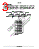
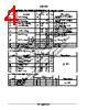
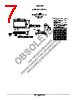
3 / 8 page  SN74LS393 http://onsemi.com 3 FUNCTIONAL DESCRIPTION Each half of the SN74LS393 operates in the Modulo 16 binary sequence, as indicated in the ÷16 Truth Table. The first flip-flop is triggered by HIGH-to-LOW transitions of the CP input signal. Each of the other flip-flops is triggered by a HIGH-to-LOW transition of the Q output of the preceding flip-flop. Thus state changes of the Q outputs do not occur simultaneously. This means that logic signals derived from combinations of these outputs will be subject to decoding spikes and, therefore, should not be used as clocks for other counters, registers or flip-flops. A HIGH signal on MR forces all outputs to the LOW state and prevents counting. SN74LS393 LOGIC DIAGRAM (one half shown) MR CP KCP J CD Q KCP J CD Q KCP J CD Q KCP J CD Q Q0 Q1 Q2 Q3 COUNT OUTPUTS Q3 Q2 Q1 Q0 0 1 2 3 4 5 6 7 8 9 10 11 L L L L H H H H H H H H L L H H L L H H L L H H L H L H L H L H L H L H L L L L L L L L H H H H 12 13 14 15 L L L L L L H H L H L H H H H H H = HIGH Voltage Level L = LOW Voltage Level TRUTH TABLE |
|
|
링크 URL |
| ALLDATASHEET 가 귀하에 도움이 되셨나요? [ DONATE ] |
Alldatasheet는? | 광고문의 | 운영자에게 연락하기 | 개인정보취급방침 | 링크 투 데이터시트 | 링크교환 | 제조사별 검색 All Rights Reserved©Alldatasheet.com |
| Russian : Alldatasheetru.com | Korean : Alldatasheet.co.kr | Spanish : Alldatasheet.es | French : Alldatasheet.fr | Italian : Alldatasheetit.com Portuguese : Alldatasheetpt.com | Polish : Alldatasheet.pl | Vietnamese : Alldatasheet.vn Indian : Alldatasheet.in | Mexican : Alldatasheet.com.mx | British : Alldatasheet.co.uk | New Zealand : Alldatasheet.co.nz |
|
Family Site : ic2ic.com |
icmetro.com |
 Korean ▼
 English
 Chinese
 German
 Japanese
 Russian
 Korean
 Spanish
 French
 Italian
 Portuguese
 Polish
 Vietnamese
 Indian
 Mexican
 British
 New Zealand