|
전자부품 데이터시트 검색엔진 |
|
|
전자부품 데이터시트 검색엔진 |
|
COP888CG 데이터시트(PDF) 20 Page - National Semiconductor (TI) |
|
|
|
|||||||||||||||||||||||||||||
COP888CG 데이터시트(HTML) 20 Page - National Semiconductor (TI) |
|
|
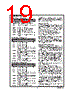
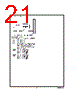
20 / 53 page  Timers (Continued) The underflows can be programmed to toggle the TxA output pin. The underflows can also be programmed to generate in- terrupts. Underflows from the timer are alternately latched into two pending flags, TxPNDA and TxPNDB. The user must reset these pending flags under software control. Two control en- able flags, TxENA and TxENB, allow the interrupts from the timer underflow to be enabled or disabled. Setting the timer enable flag TxENA will cause an interrupt when a timer un- derflow causes the RxA register to be reloaded into the timer. Setting the timer enable flag TxENB will cause an interrupt when a timer underflow causes the RxB register to be re- loaded into the timer. Resetting the timer enable flags will disable the associated interrupts. Either or both of the timer underflow interrupts may be en- abled. This gives the user the flexibility of interrupting once per PWM period on either the rising or falling edge of the PWM output. Alternatively, the user may choose to interrupt on both edges of the PWM output. Mode 2. External Event Counter Mode This mode is quite similar to the processor independent PWM mode described above. The main difference is that the timer, Tx, is clocked by the input signal from the TxA pin. The Tx timer control bits, TxC3, TxC2 and TxC1 allow the timer to be clocked either on a positive or negative edge from the TxA pin. Underflows from the timer are latched into the TxP- NDA pending flag. Setting the TxENA control flag will cause an interrupt when the timer underflows. In this mode the input pin TxB can be used as an indepen- dent positive edge sensitive interrupt input if the TxENB con- trol flag is set. The occurrence of a positive edge on the TxB input pin is latched into the TxPNDB flag. Figure 9 shows a block diagram of the timer in External Event Counter mode. Note: The PWM output is not available in this mode since the TxA pin is being used as the counter input clock. Mode 3. Input Capture Mode The device can precisely measure external frequencies or time external events by placing the timer block, Tx, in the in- put capture mode. In this mode, the timer Tx is constantly running at the fixed t c rate. The two registers, RxA and RxB, act as capture regis- ters. Each register acts in conjunction with a pin. The register RxA acts in conjunction with the TxA pin and the register RxB acts in conjunction with the TxB pin. The timer value gets copied over into the register when a trigger event occurs on its corresponding pin. Control bits, TxC3, TxC2 and TxC1, allow the trigger events to be speci- fied either as a positive or a negative edge. The trigger con- dition for each input pin can be specified independently. The trigger conditions can also be programmed to generate interrupts. The occurrence of the specified trigger condition on the TxA and TxB pins will be respectively latched into the pending flags, TxPNDA and TxPNDB. The control flag Tx- ENA allows the interrupt on TxA to be either enabled or dis- abled. Setting the TxENA flag enables interrupts to be gener- ated when the selected trigger condition occurs on the TxA pin. Similarly, the flag TxENB controls the interrupts from the TxB pin. Underflows from the timer can also be programmed to gen- erate interrupts. Underflows are latched into the timer TxC0 pending flag (the TxC0 control bit serves as the timer under- flow interrupt pending flag in the Input Capture mode). Con- sequently, the TxC0 control bit should be reset when enter- ing the Input Capture mode. The timer underflow interrupt is enabled with the TxENA control flag. When a TxA interrupt occurs in the Input Capture mode, the user must check both the TxPNDA and TxC0 pending flags in order to determine whether a TxA input capture or a timer underflow (or both) caused the interrupt. Figure 10 shows a block diagram of the timer in Input Cap- ture mode. DS012829-10 FIGURE 8. Timer in PWM Mode DS012829-11 FIGURE 9. Timer in External Event Counter Mode www.national.com 20 |
|
링크 URL |
| ALLDATASHEET 가 귀하에 도움이 되셨나요? [ DONATE ] |
Alldatasheet는? | 광고문의 | 운영자에게 연락하기 | 개인정보취급방침 | 링크 투 데이터시트 | 링크교환 | 제조사별 검색 All Rights Reserved©Alldatasheet.com |
| Russian : Alldatasheetru.com | Korean : Alldatasheet.co.kr | Spanish : Alldatasheet.es | French : Alldatasheet.fr | Italian : Alldatasheetit.com Portuguese : Alldatasheetpt.com | Polish : Alldatasheet.pl | Vietnamese : Alldatasheet.vn Indian : Alldatasheet.in | Mexican : Alldatasheet.com.mx | British : Alldatasheet.co.uk | New Zealand : Alldatasheet.co.nz |
|
Family Site : ic2ic.com |
icmetro.com |
 Korean ▼
 English
 Chinese
 German
 Japanese
 Russian
 Korean
 Spanish
 French
 Italian
 Portuguese
 Polish
 Vietnamese
 Indian
 Mexican
 British
 New Zealand