CY22381
Document #: 38-07012 Rev. *D
Page 5 of 8
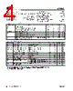
Switching Characteristics
Parameter
Name
Description
Min.
Typ.
Max.
Unit
1/t1
Output Frequency[3, 4]
Clock output limit, Commercial
–
–
200
MHz
Clock output limit, Industrial
–
–
166
MHz
t2
Output Duty Cycle[3, 5]
Duty cycle for outputs, defined as t2 ÷ t1,
Fout < 100 MHz, divider >= 2, measured
at VDD/2
45%
50%
55%
Duty cycle for outputs, defined as t2 ÷ t1,
Fout > 100 MHz or divider = 1, measured
at VDD/2
40%
50%
60%
t3
Rising Edge Slew Rate[3]
Output clock rise time, 20% to 80% of VDD
0.75
1.4
–
V/ns
t4
Falling Edge Slew Rate[3]
Output clock fall time, 20% to 80% of VDD
0.75
1.4
–
V/ns
t5
Output Three-state Timing[3]
Time for output to enter or leave
three-state mode after SHUTDOWN/OE
switches
–
150
300
ns
t6
Clock Jitter[3, 6]
Peak-to-peak period jitter, CLK outputs
measured at VDD/2
–
200
–
ps
t7
Lock Time[3]
PLL Lock Time from Power-up
–
1.0
3
ms
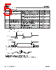
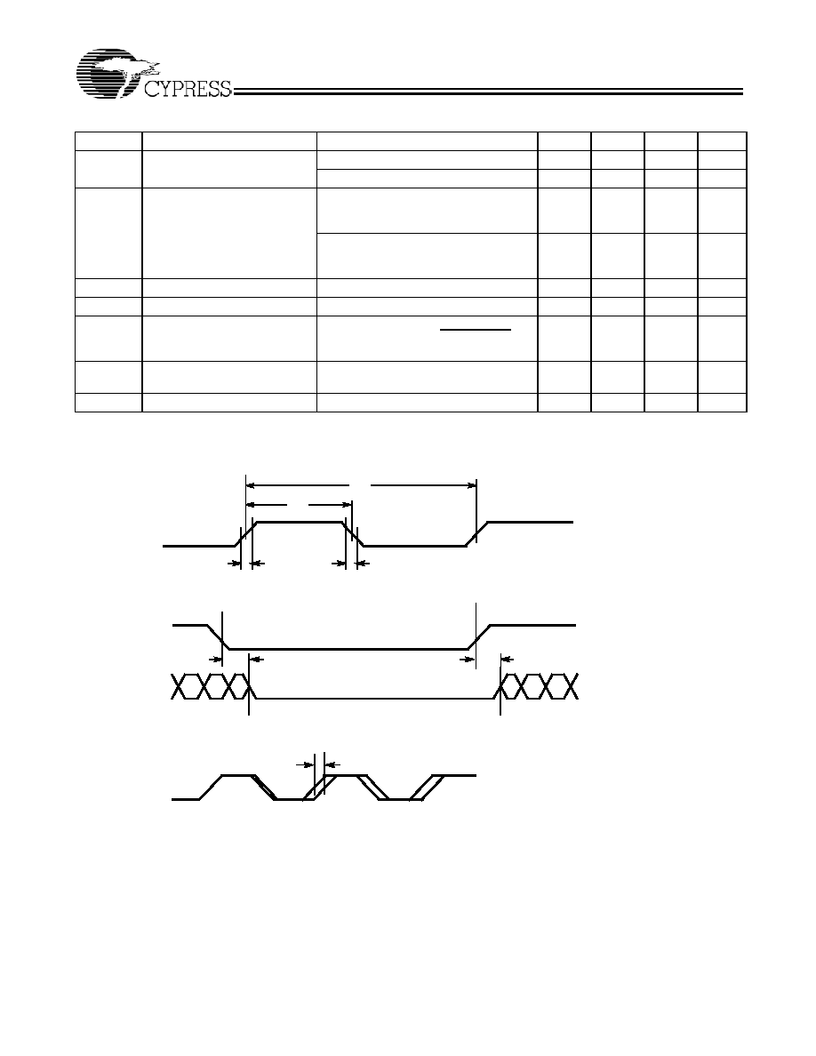
Switching Waveforms
Notes:
4. Guaranteed to meet 20% – 80% output thresholds and duty cycle specifications.
5. Reference Output duty cycle depends on XTALIN duty cycle.
6. Jitter varies significantly with configuration. Reference Output jitter depends on XTALIN jitter and edge rate.
t1
OUTPUT
t2
t3
t4
All Outputs, Duty Cycle and Rise/Fall Time
t5
OE
ALL
OUTPUTS
t5
Output Three-State Timing
THREE-STATE
CLK Output Jitter
CLK
OUTPUT
t6

 Korean ▼
 English
 Chinese
 German
 Japanese
 Russian
 Korean
 Spanish
 French
 Italian
 Portuguese
 Polish
 Vietnamese
 Indian
 Mexican
 British
 New Zealand