|
전자부품 데이터시트 검색엔진 |
|
|
전자부품 데이터시트 검색엔진 |
|
DSP56364D 데이터시트(PDF) 10 Page - Motorola, Inc |
|
|
|||||||||||||||||||||||||||||
DSP56364D 데이터시트(HTML) 10 Page - Motorola, Inc |
|
|
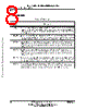
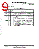
10 / 162 page  Signal/Connection Descriptions External Memory Expansion Port (Port A) 1-6 DSP56364 Advance Information MOTOROLA 1.5 EXTERNAL MEMORY EXPANSION PORT (PORT A) When the DSP56364 enters a low-power standby mode (stop or wait), it tri-states the relevant port A signals: D0–D7, AA0, AA1, RD, WR, CAS. 1.5.1 External Address Bus 1.5.2 External Data Bus Table 1-5 External Address Bus Signals Signal Name Type State during Reset Signal Description A0–A17 Output Keeper active Address Bus—A0–A17 are active-high outputs that spec- ify the address for external program and data memory accesses. Otherwise, the signals are kept to their previous values by internal weak keepers. To minimize power dissi- pation, A0–A17 do not change state when external mem- ory spaces are not being accessed. Table 1-6 External Data Bus Signals Signal Name Type State during Reset Signal Description D0–D7 Input/ Output Tri-stated Data Bus—D0–D7 are active-high, bidirectional input/out- puts that provide the bidirectional data bus for external program and data memory accesses. D0–D7 are tri-stated during hardware reset and when the DSP is in the stop or wait low-power standby mode. Freescale Semiconductor, Inc. For More Information On This Product, Go to: www.freescale.com |
|
링크 URL |
| ALLDATASHEET 가 귀하에 도움이 되셨나요? [ DONATE ] |
Alldatasheet는? | 광고문의 | 운영자에게 연락하기 | 개인정보취급방침 | 링크 투 데이터시트 | 링크교환 | 제조사별 검색 All Rights Reserved©Alldatasheet.com |
| Russian : Alldatasheetru.com | Korean : Alldatasheet.co.kr | Spanish : Alldatasheet.es | French : Alldatasheet.fr | Italian : Alldatasheetit.com Portuguese : Alldatasheetpt.com | Polish : Alldatasheet.pl | Vietnamese : Alldatasheet.vn Indian : Alldatasheet.in | Mexican : Alldatasheet.com.mx | British : Alldatasheet.co.uk | New Zealand : Alldatasheet.co.nz |
|
Family Site : ic2ic.com |
icmetro.com |
 Korean ▼
 English
 Chinese
 German
 Japanese
 Russian
 Korean
 Spanish
 French
 Italian
 Portuguese
 Polish
 Vietnamese
 Indian
 Mexican
 British
 New Zealand