|
전자부품 데이터시트 검색엔진 |
|
|
전자부품 데이터시트 검색엔진 |
|
DS1482S/T 데이터시트(PDF) 2 Page - Dallas Semiconductor |
|
|
|||||||||||||||||||||||||||||
DS1482S/T 데이터시트(HTML) 2 Page - Dallas Semiconductor |
|
|
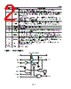
2 / 7 page  DS1482 2 of 7 PIN NAME FUNCTION 1VCCQ Operating voltage for all circuitry that connects to the controlling microprocessor (TXD, RXD, START, SPU, DONE pins). 3 SPU This line is used to control the external strong pullup function. When SPU is low, the strong pullup (PCTLZ) is high. When SPU is high and TXD is low, PCTLZ is low. 4START This line acts as an enable control for the DONE pin. If START is high, then DONE reflects the filtered digital output of the current-sense comparator. If START is low, then DONE is low. 5TXD When TXD is low, the I/O pin is pulled resistively to VCC. When TXD is high, the 1-Wire bus is pulled to GND (for write-0, write-1, read, and reset low times). 7 GND Ground Reference for VCCQ, VCC, 1-Wire 10 I/O 1-Wire Data 12 RXD This line returns the digital state of the 1-Wire bus, level-shifted to swing between VCCQ and GND. 13 DONE This line is high only when the buffered, filtered digital output from the current-sense comparator indicates that the downstream 1-Wire slave device is no longer sinking high current. This signal is enabled if START is high. 14 PCTLZ Active-low control pin for an external low-on-resistance, high-current supply. This signal typically controls the gate of a P-channel MOSFET. This signal is low when SPU is high and TXD is low. 16 VCC Operating voltage for all circuitry that connects to the 1-Wire environment (I/O and PCTLZ pins). 2, 6, 8, 9, 11, 15 N.C. Not Connected Figure 1. Block Diagram VCCQ VCC RXD TXD DONE I/O PCTLZ SPU LEVEL-SHIFT BOUNDARY START Vref + - RPUP GND |
|
|
링크 URL |
| ALLDATASHEET 가 귀하에 도움이 되셨나요? [ DONATE ] |
Alldatasheet는? | 광고문의 | 운영자에게 연락하기 | 개인정보취급방침 | 링크 투 데이터시트 | 링크교환 | 제조사별 검색 All Rights Reserved©Alldatasheet.com |
| Russian : Alldatasheetru.com | Korean : Alldatasheet.co.kr | Spanish : Alldatasheet.es | French : Alldatasheet.fr | Italian : Alldatasheetit.com Portuguese : Alldatasheetpt.com | Polish : Alldatasheet.pl | Vietnamese : Alldatasheet.vn Indian : Alldatasheet.in | Mexican : Alldatasheet.com.mx | British : Alldatasheet.co.uk | New Zealand : Alldatasheet.co.nz |
|
Family Site : ic2ic.com |
icmetro.com |
 Korean ▼
 English
 Chinese
 German
 Japanese
 Russian
 Korean
 Spanish
 French
 Italian
 Portuguese
 Polish
 Vietnamese
 Indian
 Mexican
 British
 New Zealand