|
전자부품 데이터시트 검색엔진 |
|
|
전자부품 데이터시트 검색엔진 |
|
RI-RFM-006A 데이터시트(PDF) 18 Page - Texas Instruments |
|
|
|||||||||||||||||||||||||||||
RI-RFM-006A 데이터시트(HTML) 18 Page - Texas Instruments |
|
|
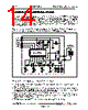
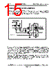
18 / 20 page  Rev. 3.5 RI-RFM-006A TIRIS RF-Module IC for Automotive Page 17 of 19 ! Precautions for Mounting and Actual Use Described in this section are the precautions to be taken at mounting and actual use of the RI-RFM-006A while designing and manufacturing a TIRIS Read-Write System using this IC, especially, critical issues as may affect the operating performance of the IC and, in particular, the system communication performance with a remote TIRIS transponder. 1. Power Supply Line When the signals returned from a remote TIRIS transponder are amplified by sequentially using the three CMOS inverter type amplifiers incorporated in this RF-module IC, an undesirable feedback loop is formed from the third amplifier toward the first one through parasitic L, R and C whose formation is not avoidable because of the structure of this IC and its internal power supply line (see the diagram below) as CMOS devices are inevitably bi-directional. If this feedback loop is left as is, it normally leads to an oscillation; particularly, when the frequency band of each amplifier is limited so that it matches that of the transponder return signals, oscillation occurs at a frequency within this band which counts on high gains from the very nature of things, in consequence, adversely affecting the demodulating performance of the received FSK signals. Equivalent circuit for internal power supply line feedback loop This situation does not a little occur when a multiple number of high-gain amplifiers are integrated in a CMOS device. Formation of this undesirable feedback loop in the amplifier band can be avoided by minimizing the impedance of the power supply line through optimization of the printed circuit boards and using a suitable bypass capacitor. It is extremely difficult to obtain true values for these parasitic L, R and C forming the internal power supply line feedback loop, but it can be said from the empirical viewpoint that it is possible to inhibit the said oscillation using a bypass capacitor with a capacity of 1 µF and having a sufficiently low impedance within the said amplifier frequency band provided that appropriate wiring patterns are defined for the power supply line on the printed circuit boards and in the peripheries of external parts for the amplifiers. Positive power supply (Vcc) line Feedback loop Bypass capacitor From Antenna 1 2 3 4 5 6 16 15 14 13 12 11 Amplifier 1 Amplifier 2 Amplifier 3 Internal power supply line |
|
|
링크 URL |
| ALLDATASHEET 가 귀하에 도움이 되셨나요? [ DONATE ] |
Alldatasheet는? | 광고문의 | 운영자에게 연락하기 | 개인정보취급방침 | 링크 투 데이터시트 | 링크교환 | 제조사별 검색 All Rights Reserved©Alldatasheet.com |
| Russian : Alldatasheetru.com | Korean : Alldatasheet.co.kr | Spanish : Alldatasheet.es | French : Alldatasheet.fr | Italian : Alldatasheetit.com Portuguese : Alldatasheetpt.com | Polish : Alldatasheet.pl | Vietnamese : Alldatasheet.vn Indian : Alldatasheet.in | Mexican : Alldatasheet.com.mx | British : Alldatasheet.co.uk | New Zealand : Alldatasheet.co.nz |
|
Family Site : ic2ic.com |
icmetro.com |
 Korean ▼
 English
 Chinese
 German
 Japanese
 Russian
 Korean
 Spanish
 French
 Italian
 Portuguese
 Polish
 Vietnamese
 Indian
 Mexican
 British
 New Zealand