|
전자부품 데이터시트 검색엔진 |
|
|
전자부품 데이터시트 검색엔진 |
|
LADLD50G-SH2-R 데이터시트(PDF) 2 Page - Unisonic Technologies |
|
|
|||||||||||||||||||||||||||||
LADLD50G-SH2-R 데이터시트(HTML) 2 Page - Unisonic Technologies |
|
|
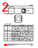
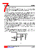
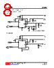
2 / 11 page  LXXLD50 CMOS IC UNISONICTECHNOLOGIESCO.,LTD 2 of 11 www.unisonic.com.tw QW-R502-474.D MARKING INFORMATION PACKAGE VOLTAGE CODE MARKING HSOP-8 25 : 2.5V AD: ADJ PIN CONFIGURATION PIN DESCRIPTION PIN NO. PIN NAME DESCRIPTION 1 GND Ground pin of the circuitry. All voltage levels are measured with respect to this pin. 2 ADJ This pin, when grounded, sets the output voltage by the internal feedback resistors; If external feedback resistors are used, the output voltage will be VOUT=0.8· (1+R1/R2) (V) where R1 is connected from VOUT to ADJ with Kelvin sensing and R2 is connected from ADJ to GND. A bypass capacitor may be connected with R1in parallel to improve load transient response. The recommended R2 and R1 are in the range of 100~10kΩ. 3 VOUT 4 VOUT Output of the regulator. Please connect Pin 3 and 4 together using wide tracks. It is necessary to connect a output capacitor with this pin for closed-loop compensation and improving transient responses. 5 VIN Main supply input pins for power conversions. The Exposed Pad provide a very low impedance input path for the main supply voltage. Please tie the Exposed Pad and VIN Pin (Pin 8) together to reduce the dropout voltage. The voltage at this pins is monitored for Power-On Reset purpose. 6 VCNTL Power input pin of the control circuitry. Connecting this pin to a +5V (recommended) supply voltage provides the bias for the control circuitry. The voltage at this pin is monitored for Power-On Reset purpose. 7 POK Power-OK signal output pin. This pin is an open-drain output used to indicate status of output voltage by sensing FB voltage. This pin is pulled low when the rising FB voltage is not above the VPOK threshold or the falling FB voltage is below the VPNOK threshold, indicating the output is not OK. 8 EN Enable control pin. Pulling and holding this pin below 0.3V shuts down the output. When re-enabled, the IC undergoes a new soft-start cycle . Left this pin open, an internal current source 10mA pulls this pin up to VCNTL voltage, enabling the regulator. |
|
|
링크 URL |
| ALLDATASHEET 가 귀하에 도움이 되셨나요? [ DONATE ] |
Alldatasheet는? | 광고문의 | 운영자에게 연락하기 | 개인정보취급방침 | 링크 투 데이터시트 | 링크교환 | 제조사별 검색 All Rights Reserved©Alldatasheet.com |
| Russian : Alldatasheetru.com | Korean : Alldatasheet.co.kr | Spanish : Alldatasheet.es | French : Alldatasheet.fr | Italian : Alldatasheetit.com Portuguese : Alldatasheetpt.com | Polish : Alldatasheet.pl | Vietnamese : Alldatasheet.vn Indian : Alldatasheet.in | Mexican : Alldatasheet.com.mx | British : Alldatasheet.co.uk | New Zealand : Alldatasheet.co.nz |
|
Family Site : ic2ic.com |
icmetro.com |
 Korean ▼
 English
 Chinese
 German
 Japanese
 Russian
 Korean
 Spanish
 French
 Italian
 Portuguese
 Polish
 Vietnamese
 Indian
 Mexican
 British
 New Zealand