|
전자부품 데이터시트 검색엔진 |
|
|
전자부품 데이터시트 검색엔진 |
|
CAT5261 데이터시트(PDF) 2 Page - Catalyst Semiconductor |
|
|
|||||||||||||||||||||||||||||
CAT5261 데이터시트(HTML) 2 Page - Catalyst Semiconductor |
|
|
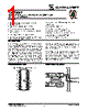
2 / 15 page  2 CAT5261 Document No. 2122, Rev. B CS is the Chip select pin. CS low enables the CAT5261 and CS high disables the CAT5261. CS high takes the SO output pin to high impedance and forces the devices into a Standby mode (unless an internal write operation is underway). The CAT5261 draws ZERO current in the Standby mode. A high to low transition on CS is required prior to any sequence being initiated. A low to high transition on CS after a valid write sequence is what initiates an internal write cycle. WP WP WP WP WP: Write Protect WP is the Write Protect pin. The Write Protect pin will allow normal read/write operations when held high. When WP is tied low, all non-volatile write operations to the Data registers are inhibited (change of wiper control register is allowed). WP going low while CS is still low will interrupt a write to the registers. If the internal write cycle has already been initiated, WP going low will have no effect on any write operation. HOLD HOLD HOLD HOLD HOLD: Hold The HOLD pin is used to pause transmission to the CAT5261 while in the middle of a serial sequence without having to re- transmit entire sequence at a later time. To pause, HOLD must be brought low while SCK is low. The SO pin is in a high imped- ance state during the time the part is paused, and transitions on the SI pins will be ignored. To resume communication, HOLD is brought high, while SCK is low. ( HOLD should be held high any time this function is not being used.) HOLD may be tied high directly to VCC or tied to VCC through a resistor. PIN DESCRIPTION Pin (SOIC/TSSOP)Name Function 1 SO Serial Data Output 2 A0 Device Address, LSB 3 NC No Connect 4 NC No Connect 5 NC No Connect 6 NC No Connect 7 VCC Supply Voltage 8RL0 Low Reference Terminal for Potentiometer 0 9RH0 High Reference Terminal for Potentiometer 0 10 RW0 Wiper Terminal for Potentiometer 0 11 CS Chip Select 12 WP Write Protection 13 SI Serial Input 14 A1 Device Address 15 RL1 Low Reference Terminal for Potentiometer 1 16 RH1 High Reference Terminal for Potentiometer 1 17 RW1 Wiper Terminal for Potentiometer 1 18 GND Ground 19 NC No Connect 20 NC No Connect 21 NC No Connect 22 NC No Connect 23 SCK Bus Serial Clock 24 HOLD Hold PIN DESCRIPTIONS SI: Serial Input SI is the serial data input pin. This pin is used to input all opcodes, byte addresses and data to be written to the CAT5261. Input data is latched on the rising edge of the serial clock. SO: Serial Output SO is the serial data output pin. This pin is used to transfer data out of the CAT5261. During a read cycle, data is shifted out on the falling edge of the serial clock. SCK: Serial Clock SCK is the serial clock pin. This pin is used to synchronize the communication between the microcontroller and the CAT5261. Opcodes, byte addresses or data present on the SI pin are latched on the rising edge of the SCK. Data on the SO pin is updated on the falling edge of the SCK. A0, A1: Device Address Inputs These inputs set the device address when address- ing multiple devices. A total of four devices can be addressed on a single bus. A match in the slave address must be made with the address input in order to initiate communication with the CAT5261. RH, RL: Resistor End Points The RH and RL pins are equivalent to the terminal connections on a mechanical potentiometer. RW: Wiper The RW pins are equivalent to the wiper terminal of a mechanical potentiometer. CS CS CS CS CS: Chip Select |
|
|
링크 URL |
| ALLDATASHEET 가 귀하에 도움이 되셨나요? [ DONATE ] |
Alldatasheet는? | 광고문의 | 운영자에게 연락하기 | 개인정보취급방침 | 링크 투 데이터시트 | 링크교환 | 제조사별 검색 All Rights Reserved©Alldatasheet.com |
| Russian : Alldatasheetru.com | Korean : Alldatasheet.co.kr | Spanish : Alldatasheet.es | French : Alldatasheet.fr | Italian : Alldatasheetit.com Portuguese : Alldatasheetpt.com | Polish : Alldatasheet.pl | Vietnamese : Alldatasheet.vn Indian : Alldatasheet.in | Mexican : Alldatasheet.com.mx | British : Alldatasheet.co.uk | New Zealand : Alldatasheet.co.nz |
|
Family Site : ic2ic.com |
icmetro.com |
 Korean ▼
 English
 Chinese
 German
 Japanese
 Russian
 Korean
 Spanish
 French
 Italian
 Portuguese
 Polish
 Vietnamese
 Indian
 Mexican
 British
 New Zealand