|
전자부품 데이터시트 검색엔진 |
|
|
전자부품 데이터시트 검색엔진 |
|
IS25LP032D-RKLE 데이터시트(PDF) 42 Page - Integrated Silicon Solution, Inc |
|
|
|||||||||||||||||||||||||||||
IS25LP032D-RKLE 데이터시트(HTML) 42 Page - Integrated Silicon Solution, Inc |
|
|
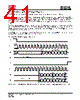
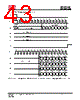
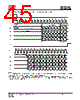
42 / 118 page  IS25LP032D IS25WP032D Integrated Silicon Solution, Inc.- www.issi.com 42 Rev. A12 08/04/2020 8.6 FAST READ QUAD OUTPUT OPERATION (FRQO, 6Bh) The FRQO instruction is used to read memory data on four output pins each at up to a 133 MHz clock. A Quad Enable (QE) bit of Status Register must be set to "1" before sending the Fast Read Quad Output instruction. The FRQO instruction code is followed by three address bytes (A23 – A0) and dummy cycles (configurable, default is 8 clocks), transmitted via the IO0 line, with each bit latched-in during the rising edge of SCK. Then the first data byte addressed is shifted out on the IO3, IO2, IO1 and IO0 lines, with each group of four bits shifted out at a maximum frequency fCT, during the falling edge of SCK. The first bit (MSB) is output on IO3, while simultaneously the second bit is output on IO2, the third bit is output on IO1, etc. The first byte addressed can be at any memory location. The address is automatically incremented after each byte of data is shifted out. When the highest address is reached, the address counter will roll over to the 000000h address, allowing the entire memory to be read with a single FRQO instruction. FRQO instruction is termin ated by driving CE# high (VIH). If a FRQO instruction is issued while an Erase, Program or Write cycle is in process (BUSY=1) the instruction is ignored and will not have any effects on the current cycle. |
|
링크 URL |
| ALLDATASHEET 가 귀하에 도움이 되셨나요? [ DONATE ] |
Alldatasheet는? | 광고문의 | 운영자에게 연락하기 | 개인정보취급방침 | 링크 투 데이터시트 | 링크교환 | 제조사별 검색 All Rights Reserved©Alldatasheet.com |
| Russian : Alldatasheetru.com | Korean : Alldatasheet.co.kr | Spanish : Alldatasheet.es | French : Alldatasheet.fr | Italian : Alldatasheetit.com Portuguese : Alldatasheetpt.com | Polish : Alldatasheet.pl | Vietnamese : Alldatasheet.vn Indian : Alldatasheet.in | Mexican : Alldatasheet.com.mx | British : Alldatasheet.co.uk | New Zealand : Alldatasheet.co.nz |
|
Family Site : ic2ic.com |
icmetro.com |
 Korean ▼
 English
 Chinese
 German
 Japanese
 Russian
 Korean
 Spanish
 French
 Italian
 Portuguese
 Polish
 Vietnamese
 Indian
 Mexican
 British
 New Zealand