|
전자부품 데이터시트 검색엔진 |
|
|
전자부품 데이터시트 검색엔진 |
|
IS25LP032D-RGLA3 데이터시트(PDF) 82 Page - Integrated Silicon Solution, Inc |
|
|
|||||||||||||||||||||||||||||
IS25LP032D-RGLA3 데이터시트(HTML) 82 Page - Integrated Silicon Solution, Inc |
|
|
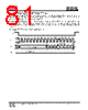
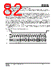
82 / 118 page  IS25LP032D IS25WP032D Integrated Silicon Solution, Inc.- www.issi.com 82 Rev. A12 08/04/2020 8.37 INFORMATION ROW PROGRAM OPERATION (IRP, 62h) The Information Row Program (IRP) instruction allows up to 256 bytes data to be programmed into the memory in a single operation. Before the execution of IRP instruction, the Write Enable Latch (WEL) must be enabled through a Write Enable (WREN) instruction. The IRP instruction code, three address bytes and program data (1 to 256 bytes) should be sequentially input. Three address bytes has to be input as specified in the Table 8.7 Information Row Valid Address Range. Program operation will start once the CE# goes high, otherwise the IRP instruction will not be executed. The internal control logic automatically handles the programming voltages and timing. The progress or completion of the program operation can be determined by reading the WIP bit in Status Register via a RDSR instruction. If the WIP bit is “1”, the program operation is still in progress. If WIP bit is “0”, the program operation has completed. If more than 256 bytes data are sent to a device, the address counter rolls over within the same page. The previously latched data are discarded and the last 256 bytes data are kept to be programmed into the page. The starting byte can be anywhere within the page. When the end of the page is reached, the address will wrap around to the beginning of the same page. If the data to be programmed are less than a full page, the data of all other bytes on the same page will remain unchanged. Note: A program operation can alter “1”s into “0”s, The same byte location or Information Row array may be programmed more than once to incrementally change “1” to “0”s. An erase operation is required to change “0”s back to “1”s. Figure 8.61 IRP (Information Row Program) Sequence Instruction = 62h 23 CE # SCK SI 7 6 SO 7 3-byte Address High Impedance 22 ... 0 Data In 1 Data In 256 0 1 ... 7 8 9 ... 31 32 33 ... 39 ... ... Mode 3 Mode 0 ... 0 ... ... 0 |
|
링크 URL |
| ALLDATASHEET 가 귀하에 도움이 되셨나요? [ DONATE ] |
Alldatasheet는? | 광고문의 | 운영자에게 연락하기 | 개인정보취급방침 | 링크 투 데이터시트 | 링크교환 | 제조사별 검색 All Rights Reserved©Alldatasheet.com |
| Russian : Alldatasheetru.com | Korean : Alldatasheet.co.kr | Spanish : Alldatasheet.es | French : Alldatasheet.fr | Italian : Alldatasheetit.com Portuguese : Alldatasheetpt.com | Polish : Alldatasheet.pl | Vietnamese : Alldatasheet.vn Indian : Alldatasheet.in | Mexican : Alldatasheet.com.mx | British : Alldatasheet.co.uk | New Zealand : Alldatasheet.co.nz |
|
Family Site : ic2ic.com |
icmetro.com |
 Korean ▼
 English
 Chinese
 German
 Japanese
 Russian
 Korean
 Spanish
 French
 Italian
 Portuguese
 Polish
 Vietnamese
 Indian
 Mexican
 British
 New Zealand