|
전자부품 데이터시트 검색엔진 |
|
|
전자부품 데이터시트 검색엔진 |
|
PLL650-05SC-R 데이터시트(PDF) 3 Page - PhaseLink Corporation |
|
|
|||||||||||||||||||||||||||||
PLL650-05SC-R 데이터시트(HTML) 3 Page - PhaseLink Corporation |
|
|
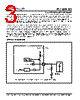
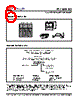
3 / 6 page  PLL650-05 Low EMI Network LAN Clock 47745 Fremont Blvd., Fremont, California 94538 Tel (510) 492-0990 Fax (510) 492-0991 www.phaselink.com Rev 09/03/04 Page 3 since the pin also needs to serve as output. In the case of two level input pins, an internal pull-up resistor is present. This allows a default value to be set when no external pull down resistor is connected between the pin and GND (by definition, a tri-level input has a the default value of "M" (mid) if it is not connected). In order to connect a bi-directional pin to a non-default value, the input must be connected to GND or VDD through an external pull-down/pull-up resistor. Note: when the output load presents a low impedance in comparison to the internal pull-up resistor, the internal pull-up resistor may not be sufficient to pull the input up to a logical “one”, and an external pull-up resistor may be required. For bi-directional inputs, the external loading resistor between the pin and GND has to be sufficiently small (compared to the internal pull-up resistor) so that the pin voltage be pulled below 0.8V (logical “zero”). In order to avoid loading effects when the pin serves as output, the value of the external pull-down resistor should however be kept as large as possible. In general, it is recommended to use an external resistor of around one sixth to one quarter of the internal pull-up resistor (see Application Diagram). Note: when the output is used to drive a load presenting an small resistance between the output pin and VDD, this resistance is in essence connected in parallel to the internal pull-up resistor. In such a case, the external pull-down resistor may have to be dimensioned smaller to guarantee that the pin voltage will be low enough achieve the desired logical “zero”. This is particularly true when driving 74FXX TTL components. APPLICATION DIAGRAM Latch Power Up Reset Jumper options R UP/4 Clock Load Latched Input Output EN VDD R up Bi-directional pin R RB NOTE: Rup=120k Ω for 50MHz_OE (Pin2); Rup=60k Ω for FS(0:1). R starts from 1 to 0 while RB starts from 0 to 1. Internal to chip External Circuitry |
|
|
링크 URL |
| ALLDATASHEET 가 귀하에 도움이 되셨나요? [ DONATE ] |
Alldatasheet는? | 광고문의 | 운영자에게 연락하기 | 개인정보취급방침 | 링크 투 데이터시트 | 링크교환 | 제조사별 검색 All Rights Reserved©Alldatasheet.com |
| Russian : Alldatasheetru.com | Korean : Alldatasheet.co.kr | Spanish : Alldatasheet.es | French : Alldatasheet.fr | Italian : Alldatasheetit.com Portuguese : Alldatasheetpt.com | Polish : Alldatasheet.pl | Vietnamese : Alldatasheet.vn Indian : Alldatasheet.in | Mexican : Alldatasheet.com.mx | British : Alldatasheet.co.uk | New Zealand : Alldatasheet.co.nz |
|
Family Site : ic2ic.com |
icmetro.com |
 Korean ▼
 English
 Chinese
 German
 Japanese
 Russian
 Korean
 Spanish
 French
 Italian
 Portuguese
 Polish
 Vietnamese
 Indian
 Mexican
 British
 New Zealand