|
전자부품 데이터시트 검색엔진 |
|
|
전자부품 데이터시트 검색엔진 |
|
7708 데이터시트(PDF) 21 Page - Power Integrations, Inc. |
|
|
|||||||||||||||||||||||||||||
7708 데이터시트(HTML) 21 Page - Power Integrations, Inc. |
|
|
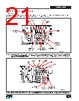
21 / 42 page  Rev. B 04/15 21 TFS7701-7708 www.power.com Figure 24. LINE-SENSE and RESET Pin Resistor Layout. The 2 Resistors Connected to LINSE-SENSE and RESET Pins Should be SMD, and the GROUND and BYPASS Pin Traces Provide Faraday Shielding Against the HIGH-SIDE SOURCE and MAIN-DRAIN Pin Traces. The Bypass Capacitor is Through-Hole Type so that the Traces Connecting to the Pins can be Very Short. Figure 25. Layout Around ENABLE and FEEDBACK Pin. Use Quiet Traces as Faraday Shields from Noisy Traces, Especially if the Traces to the Optocouplers are Long. Transformer Secondary and Output Diodes Flyback Layout The diode and output capacitor should be mounted close to the secondary winding and routed with short traces. The standby PI-7012-052113 GROUND Pin RESET Pin LINE-SENSE Pin BYPASS Pin LINE-SENSE AND RESET Pin Resistors (SMD) High-Side Source Trace (Noisy) GROUND Pin Trace Acting as Shield MAIN DRAIN Pin (Noisy) Bypass Capacitor BYPASS Pin Trace Acting as Shield PI-7022-052113 DSB (Noisy) Ground (Shield) ENABLE Pin High-Side Drain (Quiet) VAUX (Quiet) VDDH Parts (Noisy) Bootsrap Diode Placed Near VDDH High-Side Source (Noisy) FEEDBACK Pin primary bias (V AUX ) capacitor and diode should be mounted close to the winding. |
|
링크 URL |
| ALLDATASHEET 가 귀하에 도움이 되셨나요? [ DONATE ] |
Alldatasheet는? | 광고문의 | 운영자에게 연락하기 | 개인정보취급방침 | 링크 투 데이터시트 | 링크교환 | 제조사별 검색 All Rights Reserved©Alldatasheet.com |
| Russian : Alldatasheetru.com | Korean : Alldatasheet.co.kr | Spanish : Alldatasheet.es | French : Alldatasheet.fr | Italian : Alldatasheetit.com Portuguese : Alldatasheetpt.com | Polish : Alldatasheet.pl | Vietnamese : Alldatasheet.vn Indian : Alldatasheet.in | Mexican : Alldatasheet.com.mx | British : Alldatasheet.co.uk | New Zealand : Alldatasheet.co.nz |
|
Family Site : ic2ic.com |
icmetro.com |
 Korean ▼
 English
 Chinese
 German
 Japanese
 Russian
 Korean
 Spanish
 French
 Italian
 Portuguese
 Polish
 Vietnamese
 Indian
 Mexican
 British
 New Zealand