|
전자부품 데이터시트 검색엔진 |
|
|
전자부품 데이터시트 검색엔진 |
|
M24C16-R 데이터시트(PDF) 11 Page - STMicroelectronics |
|
|
|||||||||||||||||||||||||||||
M24C16-R 데이터시트(HTML) 11 Page - STMicroelectronics |
|
|
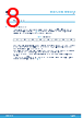
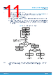
11 / 40 page  5.1.3 Minimizing write delays by polling on ACK The maximum write time (tw) is shown in AC characteristics tables in Section 8 DC and AC parameters, but the typical time is shorter. To make use of this, a polling sequence can be used by the bus master. The sequence, as shown in Figure 8, is: • Initial condition: a write cycle is in progress. • Step 1: the bus master issues a Start condition followed by a device select code (the first byte of the new instruction). • Step 2: if the device is busy with the internal write cycle, no ACK is returned and the bus master goes back to step 1. If the device has terminated the internal write cycle, it responds with an ACK, indicating that the device is ready to receive the second part of the instruction (the first byte of this instruction having been sent during Step 1). Figure 8. Write cycle polling flowchart using ACK Write cycle in progress Next operation is addressing the memory Start condition ACK returned YES NO YES NO Re-start Stop Data for the write operation Send address and receive ACK YES NO Continue the write operation Continue the random read operation Device select with RW = 1 First byte of instruction with RW = 0 already decoded by the device Device select with RW = 0 StartCondition Note: The seven most significant bits of the device select code of a random read (bottom right box in the figure)must be identical to the seven most significant bits of the device select code of the write (polling instruction in the figure). M24C16-W M24C16-R M24C16-F Write operations DS9194 - Rev 11 page 11/40 |
|
링크 URL |
| ALLDATASHEET 가 귀하에 도움이 되셨나요? [ DONATE ] |
Alldatasheet는? | 광고문의 | 운영자에게 연락하기 | 개인정보취급방침 | 링크 투 데이터시트 | 링크교환 | 제조사별 검색 All Rights Reserved©Alldatasheet.com |
| Russian : Alldatasheetru.com | Korean : Alldatasheet.co.kr | Spanish : Alldatasheet.es | French : Alldatasheet.fr | Italian : Alldatasheetit.com Portuguese : Alldatasheetpt.com | Polish : Alldatasheet.pl | Vietnamese : Alldatasheet.vn Indian : Alldatasheet.in | Mexican : Alldatasheet.com.mx | British : Alldatasheet.co.uk | New Zealand : Alldatasheet.co.nz |
|
Family Site : ic2ic.com |
icmetro.com |
 Korean ▼
 English
 Chinese
 German
 Japanese
 Russian
 Korean
 Spanish
 French
 Italian
 Portuguese
 Polish
 Vietnamese
 Indian
 Mexican
 British
 New Zealand