|
전자부품 데이터시트 검색엔진 |
|
|
전자부품 데이터시트 검색엔진 |
|
C5EC3EARCH-RM/D 데이터시트(PDF) 79 Page - NXP Semiconductors |
|
|
|||||||||||||||||||||||||||||
C5EC3EARCH-RM/D 데이터시트(HTML) 79 Page - NXP Semiconductors |
|
|
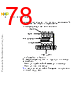
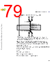
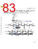
79 / 114 page  Power and Thermal Characteristics 79 03 Figure 11 Package with Heat Sink Mounted to the Printed Circuit Board Heat generated on the active side of the chip is conducted through the silicon, then through the heat sink attach material (or thermal interface material), and finally to the heat sink where it is removed by convection. Because the silicon thermal resistance is quite small, for a first-order analysis, the temperature drop in the silicon may be neglected. Thus, the thermal interface material and the heat sink conduction/convective thermal resistances are the dominant terms. Heat Sink Selection Example For preliminary heat sink sizing, the die-junction temperature can be expressed as follows: T j = T a + T r + (θjc + θint + θsa ) x P d where: T j is the die-junction temperature T a is the inlet cabinet ambient temperature T r is the air temperature rise within the computer cabinet External Resistance Internal Resistance External Resistance Radiation Heat Sink Printed Circuit Board (PCB) Radiation Convection Thermal Interface Material Die/Package Die Junction Package/Leads Convection Freescale Semiconductor, Inc. For More Information On This Product, Go to: www.freescale.com |
|
링크 URL |
| ALLDATASHEET 가 귀하에 도움이 되셨나요? [ DONATE ] |
Alldatasheet는? | 광고문의 | 운영자에게 연락하기 | 개인정보취급방침 | 링크 투 데이터시트 | 링크교환 | 제조사별 검색 All Rights Reserved©Alldatasheet.com |
| Russian : Alldatasheetru.com | Korean : Alldatasheet.co.kr | Spanish : Alldatasheet.es | French : Alldatasheet.fr | Italian : Alldatasheetit.com Portuguese : Alldatasheetpt.com | Polish : Alldatasheet.pl | Vietnamese : Alldatasheet.vn Indian : Alldatasheet.in | Mexican : Alldatasheet.com.mx | British : Alldatasheet.co.uk | New Zealand : Alldatasheet.co.nz |
|
Family Site : ic2ic.com |
icmetro.com |
 Korean ▼
 English
 Chinese
 German
 Japanese
 Russian
 Korean
 Spanish
 French
 Italian
 Portuguese
 Polish
 Vietnamese
 Indian
 Mexican
 British
 New Zealand