|
전자부품 데이터시트 검색엔진 |
|
|
전자부품 데이터시트 검색엔진 |
|
DFE252012F-R47M 데이터시트(PDF) 7 Page - Analog Devices |
|
|
|||||||||||||||||||||||||||||
DFE252012F-R47M 데이터시트(HTML) 7 Page - Analog Devices |
|
|
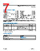
7 / 122 page  Absolute Maximum Ratings SYS to AGND ...................................................... -0.3V to +17.6V ALT_IN to AGND ................................................... -0.3V to +6.0V VDD to AGND ........................................................ -0.3V to +2.2V VL12, VL34 to AGND, PGND ................................. -0.3V to +2.2V CE to AGND ........................... -0.3V to min (VSYS + 0.3, +17.6)V CFGx to AGND........................... -0.3V to min (VDD + 0.3, +2.2)V SELx to AGND ........................... -0.3V to min (VDD + 0.3, +2.2)V INx to PGNDx, AGND.......................................... -0.3V to +17.6V LXx to PGNDx ..................................................... -0.3V to +17.6V LXx to PGNDx (less than 10ns) .................... (VIN - 22)V to +22V BSTx to LXx .......................................................... -0.3V to +2.2V SNSxP to AGND ................................................. -0.3V to +12.0V SNSxN to AGND.................................................... -0.3V to +0.3V PGNDx to AGND ................................................... -0.3V to +0.3V VIO to AGND.......................................................... -0.3V to +2.2V SCL to AGND......................................................... -0.3V to +2.2V SDA to AGND ........................................................ -0.3V to +2.2V IRQB to AGND....................................................... -0.3V to +2.2V MFIOx to AGND...........................-0.3V to min (VIO + 0.3, +2.2)V Continuous Power Dissipation (JESD51-7, TA = +70ºC) 60 WLP (derate 25.4mW/°C above +70°C).................2037mW Junction Temperature ....................................................... +150°C Storage Temperature Range ..............................-65°C to +150°C Soldering Temperature (reflow) ........................................+260°C Note 1: LXx has internal clamp diodes to its corresponding PGNDx and INx. Applications that forward bias these diodes should take care not to exceed the IC's package power dissipation limits. Stresses beyond those listed under “Absolute Maximum Ratings” may cause permanent damage to the device. These are stress ratings only, and functional operation of the device at these or any other conditions beyond those indicated in the operational sections of the specifications is not implied. Exposure to absolute maximum rating conditions for extended periods may affect device reliability. Recommended Operating Conditions PARAMETER SYMBOL CONDITION TYPICAL RANGE UNIT Input Voltage Range VIN 2.8 to 16 V Output Current Range IOUT For continuous operation at 4A, the junction temperature (TJ) is limited to +120ºC; if the junction temperature is higher than +120ºC, the expected lifetime at 4A continuous operation is derated 0 to 4 A Junction Temperature Range TJ -40 to +125 ºC Note: These limits are not guaranteed. Package Information 60 WLP (Thick UBM) Packkage Code W602A4Z+1 Outline Number 21-100610 Land Pattern Number Application Note 1891 Thermal Resistance, Four-Layer Board: Junction-to-Ambient (θJA) 39.27°C/W MAX77542 16VIN/16A, Quad-Phase High-Efficiency Buck Converter www.analog.com Analog Devices | 7 |
|
링크 URL |
| ALLDATASHEET 가 귀하에 도움이 되셨나요? [ DONATE ] |
Alldatasheet는? | 광고문의 | 운영자에게 연락하기 | 개인정보취급방침 | 링크 투 데이터시트 | 링크교환 | 제조사별 검색 All Rights Reserved©Alldatasheet.com |
| Russian : Alldatasheetru.com | Korean : Alldatasheet.co.kr | Spanish : Alldatasheet.es | French : Alldatasheet.fr | Italian : Alldatasheetit.com Portuguese : Alldatasheetpt.com | Polish : Alldatasheet.pl | Vietnamese : Alldatasheet.vn Indian : Alldatasheet.in | Mexican : Alldatasheet.com.mx | British : Alldatasheet.co.uk | New Zealand : Alldatasheet.co.nz |
|
Family Site : ic2ic.com |
icmetro.com |
 Korean ▼
 English
 Chinese
 German
 Japanese
 Russian
 Korean
 Spanish
 French
 Italian
 Portuguese
 Polish
 Vietnamese
 Indian
 Mexican
 British
 New Zealand